Plasmonic metasurfaces are a promising technology for use in reflective display applications. Reasons for this include the ability of this approach to produce pixels that can have a wide color gamut and a high spatial resolution. Unfortunately, up to now, the use of plasmonic technology has not been successfully commercialized because it does not readily allow for color tuning.

In addition, implementation of the approach requires the use of expensive nano lithographic fabrication techniques. Addressing these issues has been the subject of a team of researchers working in the NanoPhotonics Centre within the Cavendish Laboratory at the University of Cambridge (Cambridge, UK) and led by Jialong Peng.
A recent article on this topic by the researchers was published in Science Advances 10 May 2019:Vol. 5, no. 5, eaaw2205. A copy of the article is available for download here.
First, a few words of background information. Paraphrasing definitions in found in Wikipedia:
- A metasurface refers to a kind of artificial sheet material with sub-wavelength thickness. Metasurfaces can be either structured or unstructured with subwavelength-scaled patterns in the horizontal dimensions. In electromagnetic theory, metasurfaces modulate the behaviors of electromagnetic waves through specific boundary conditions.
- Plasmonic nanoparticles are particles whose electron density can couple with electromagnetic radiation of wavelengths that are far larger than the particle due to the nature of the dielectric-metal interface between the medium and the particles.
Active plasmonic colors can be obtained when the optical properties of the surrounding media are controlled by an applied stimulus. “Plasmonic metasurfaces combined with electrochromic materials, including conductive polymers and phase change materials, typically show on/off switching when the charge state of the electrochromic material changes.”
The variation of this approach investigated by the team in their most current research was based on the use of a multilayered plasmonic composite architecture. In this variation, the plasmonic gap is filled with an active dielectric spacer of electrochromic nanoparticles.
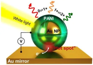
More specifically, the researchers used electrochromic NanoParticle-on-Mirror constructs (eNPoMs) formed from gold nanoparticles (NPs) encapsulated in a conductive polymer shell composed of PolyANIline (PANI). The shell has a thickness up to about 20 nm. The particles are coated onto a gold (Au) mirror.
The key feature of this approach is that “the nanoparticles strongly confine light within their individual gaps to the underlying mirror and thus produce extremely localized cavity resonances.” This, in turn, makes the reflection insensitive to the angle and polarization of the incident light. Color is controlled by switching the charge state (that is, the redox state) of the entire PANI shell, thus rapidly shifting the resonant scattering color of the eNPoM.
The graphic in the figure below illustrates the structure and functioning of the eNPoM.
Schematic of an eNPoM, which changes color as a function of redox state of the thin PANI shell surrounding each Au NP on an Au mirror substrate.
A particular feature of this approach is that such a device can be constructed by “lithography-free” methods to subnanometer precision.
During tests, the nanopixels demonstrated:
- Strong, uniform, nonfading scattering colors.
- An optical contrast greater than 50%.
- Bistable behavior with persistence times exceeding hundreds of seconds.
- The ability to be electrically tuned across greater than 100 nm wavelength ranges.
- Energy consumption rates of 9 fJ per pixel. (That is, active nanopixels required about 0.2 fJ of energy for each 1 nm shift in wavelength.)
- A refresh rate greater than 50 Hz, adequate for commercial video applications.
One particularly significant point is that these performance characteristics are reported to scale from the single nanoparticle level to multicentimeter sized films – and to do so in devices that have a sub-wavelength thickness.
In their article, the researchers conclude by stating that their approach shows “vivid uniform color dynamics, not possible with any existing plasmonic color system.” -Arthur Berman
NanoPhotonics Centre, Jialong Peng, [email protected]

