A team of researchers from the Korea Advanced Institute of Science and Technology or KAIST and the Electronics and Telecommunications Research Institute or ETRI (both located in Daejeon, Republic of Korea) are developing a new metal oxide charge transfer complex that, when dispersed into the stack of an OLED, can improve device efficiency.
Here is some background information on this development. The explanation has been paraphrased from the technical article cited below.
Metal oxide thin films have a favorable energy band structure, excellent processability and high stability. Due to these desirable properties, material systems of this type have been successfully used in multi-layered optoelectronic devices such as OLEDs. The reason for using such material systems is to ensure meeting the twin goals of efficient charge transport and efficient charge injection into the emission layer. Up to now, the designs of conventional devices using this approach have usually been based on the use of pristine metal oxides. The reason for choosing this approach is the fact that such materials have electrical properties that are compatible with those of the target active layer. However, with the advent of new active layer materials and the demand for higher device performance, pristine metal oxide systems have been found unable to fully meet desired goals.
What is the problem? The charge transport and the charge injection properties of metal oxide thin film based devices are typically determined by two factors – the charge carrier density of each layer and the configuration of the energy levels. Although the values of these two factors can be enhanced by adjusting the compositions of the materials, it has proven difficult using conventional techniques to achieve enhancement of both properties simultaneously and throughout the entire metal oxide layer.
To address these issues, the team investigated the use of a heterostructure based metal oxide charge transfer complex. The complex was composed of two complementary metal oxides that served to modulate both the energy levels and the electrical conductivities. The modulation is accomplished by inducing effective charge transfer between the two metal oxides. More specifically, the approach was designed to widen the charge transfer range from the localized interface to the whole film. This, in turn, was accomplished by forming a nanodomain dispersed heterostructure that produces a distinct energy band structure at the nanoscale.
A recent article by the team on this topic is entitled “Metal oxide charge transfer complex for effective energy band tailoring in multilayer optoelectronics.” It was published in Nat Commun 13, 75 (2022) and can be found on line here.
In their article, the researchers describe the specifics of their new approach. Here are a few of the top level details. The material was made from nickel oxide as a p-type matrix and molybdenum oxide nanoparticles. A NiO:MoO3 complex, made from nanometer sized MoO3 domains was used as a strong p-type dopant embedded in NiO matrices. In the NiO:MoO3 complex, the energy levels can be controlled by varying the fraction of MoO3 nanoparticles in the complex. This is possible because it is the total interfacial area that defines the extent of charge transfer. Experimental analyses revealed clearly distinct NiO and MoO3 phases, suggesting that their individual energy structures are maintained at the nanoscale.
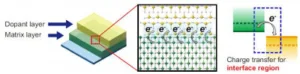
The figure below illustrates several features of the new heterostructure charge transfer complex formation approach.
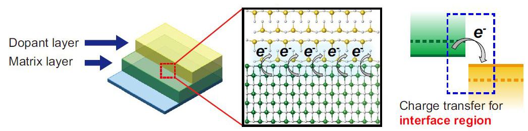 Schematic of metal oxide material system and a representative energy level diagram for the heterostructure charge transfer complex formation that is the basis of the approach under development by the research team.
Some of the experimental results reported in the article are as follows:
- The NiO and MoO3work function could be modulated between 4.47 to 6.34?eV.
- The electrical conductivity was enhanced by a factor of 2.4 compared to that of pristine NiO.
- The current efficiency in a test green phosphorescent OLED utilizing NiO:MoO3 presented 43% and 189% higher current efficiency than that of pristine NiO and MoO3
- A test blue phosphorescent OLED utilizing NiO:MoO3 demonstrated excellent current efficiency of 32.6?cd/A and external quantum efficiency of 17%.
In their article, the researchers represent that their new approach demonstrates an ability to overcome the limitations of conventional metal oxide enhancement methods. The ability to do so is accomplished by delocalizing charge transfer from the surface to the entire film. The researchers conclude their article by suggesting that the new approach represents “an alternative direction for applying metal oxide heterostructures to enhance the performance of multi-layered optoelectronic devices.” -Arthur Berman
KAIST, Yeon Sik Jung, [email protected]