 Professor Hiroshi Amano was the third keynote speaker at DisplayWeek and he discussed Nanorod LEDs in the display field. However, he started by pointing out the contribution of LEDs in reducing power use in applications such as lighting. Low power lighting can make a dramatic impact on development in many areas of the world where mains power is not available. There are many applications for LED and he showed a roadmap for the development of devices and applications.
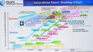
D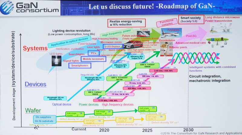 Gan Roadmap – click for higher resolution. Image:Meko
Amano is working in a development lab in Japan that has many facilities ‘under one roof’ for the development of LEDs. The group has collaboration with researchers in Korea as well.
There is a problem with LEDs when they get below 10µm per side as then the external quantum efficiency drops because of surface recombination at the side wall. That means that a new approach is needed and he favours Gallium Nitride (GaN) nanorods. Higher efficiency is needed for 8K displays because of the low efficiency of current LCDs.
He believes that this technology is likely to become an option for display use in the future. This is especially when the display resolution of future consumer electronics products is required to increase to 8K. The chip dimension of MicroLEDs should be smaller than 1?m so as to match with the display of a cellphone with extremely high resolution. Whether quantum dots or phosphor is used to convert from blue LED light, either will face a big technical obstacle to achieving a coating that will achieve color conversion on such a tiny chip. (We have already reported that particles of traditional phosphor are already too big for really small microLEDs)
Certainly, such technology will not be appropriate for the existing LED production process, so the equipment that grows the epitaxial wafer is required to be modified. However, as for the mode of growing an appropriate epi wafer structure, a structure with dissimilar materials should be slowly grown through what he called “the interlace mode between injection and interruption”. The intention of the process is to achieve RGB full-color light from one wafer. Then, when can the production of this highly advanced technology come true? Let’s hope to see it during our lifetime, Amano said.
To make something like the Cledis concept for wearable display applications, the LED should be less than 1 micron on each side. Sony’s Cledis is great, Amano said, but it’s just too big for many applications. The power efficiency, considering the high quality is good, however.
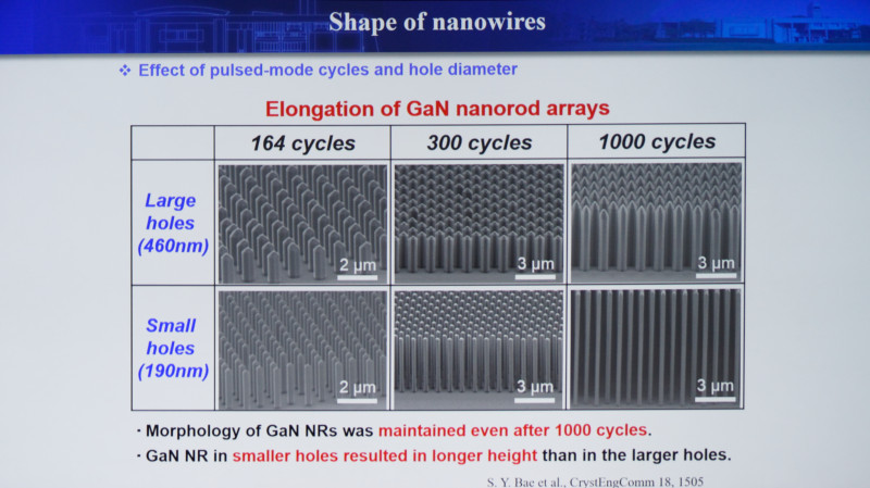
Nanorod LEDs can be made much smaller than traditional LEDs and can be made using MOVPE, although carbon can get in which causes a problem. Because of this, it’s best to use a pulse mode, Amano said. He then went through some of the manufacturing processes.
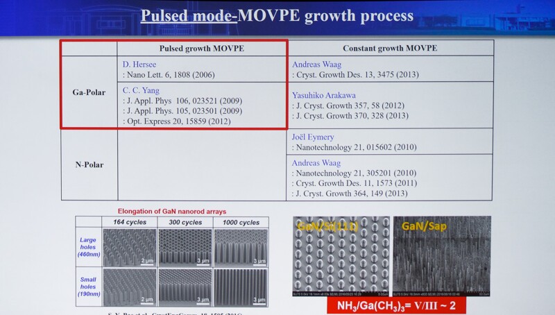 MOVPE can be used to make Nanorods. Click for higher resolution. Image:Meko
Phosphor particles are bigger than the rods – but with QD phosphor it will be very hard to get a good black, Amano said (presumably because of the problem of photon-driven emission).
You can control the wavelength of the light from quantum rods with the height of the rod and with indium incorporation. So you can make RGB using the same substrate and process. The shape of the rod can be controlled to allow the emission of four different wavelengths of light. The balance between the colours is controlled by the current applied.
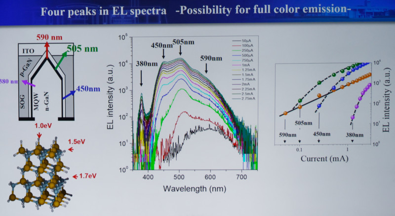 Light is emitted at different frequencies with the balance controlled by the current. Image:Meko
At the moment, the green being produced is a blueish colour and the red is really orange, so more development is needed.
The key point is that you may be able to make all colours with a single architecture, he concluded.