For most of the past decade, the story of OLED advancement has been told in nits and color volumes, with each generation of panels from Samsung Display and LG Display pushing peak brightness and gamut coverage to new records. At MWC 2026, Visionox offered a different kind of argument: that the bottleneck holding OLED back is no longer what a panel can do at its best, but whether the process that makes it can scale reliably, cost-effectively, and into form factors that a fine metal mask cannot reach.
The panel maker arrived in Barcelona with two centerpiece technologies, one addressing how pixels are formed and the other addressing the chemistry that makes them emit light. Taken together, they sketch a manufacturing-materials roadmap that is deliberately positioned around the demands of AI-driven devices, where displays are increasingly expected to stay active longer, render more information, and do it all within tighter system power envelopes.
Retiring the Fine Metal Mask
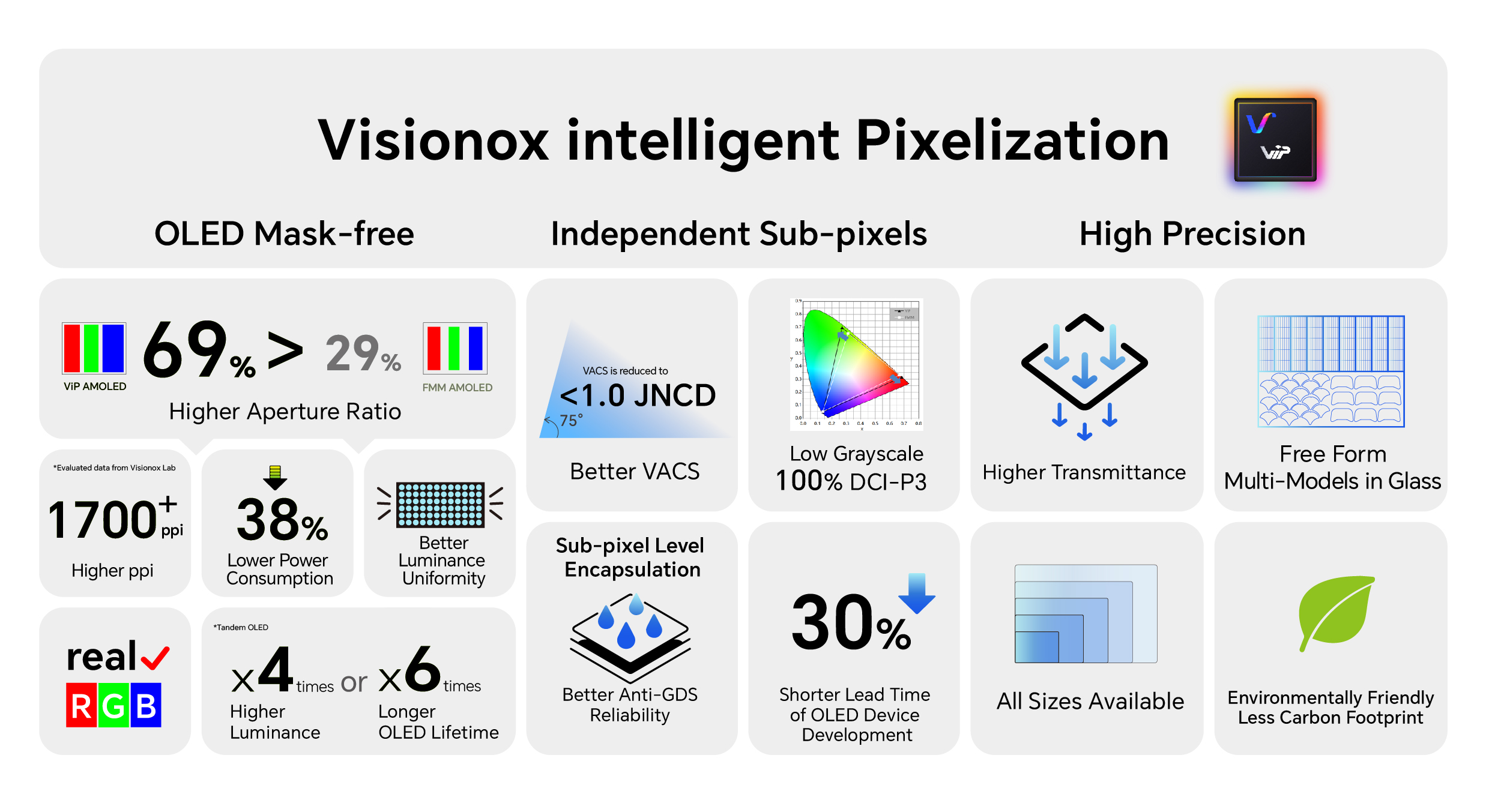
Fine metal masks, the stencils used to deposit OLED emissive materials onto substrates with the precision needed for high-resolution pixel patterns, have been a production staple for two decades. They have also been, for much of that time, an engineering constraint. As pixel densities push past 500 ppi for high-end smartphones and toward the thousands for near-eye displays, the masks themselves become increasingly difficult to handle. At very fine pitches, they sag and distort. At large substrate sizes, alignment tolerances compound. The result is an aperture ratio, the fraction of each pixel that actually emits light, typically stuck around 29% in conventional AMOLED production.
| Company | Pixel tech in mass productiony | Patterning method | Stand‑out strengths | Key gaps / risks |
|---|---|---|---|---|
| Visionox (ViP) | ViP RGB AMOLED (phones, high‑PPI prototypes) | Photolithography (FMM‑free) | Huge aperture gain, very high PPI, strong power/lifetime story | New process, cost/yield still being proven at real volume |
| Samsung Display | LTPO/FMM OLED, QD‑OLED with V‑stripe | FMM (mobile), non‑RGB for QD‑OLED | Peak brightness, mature yields, deep OEM ties | Still dependent on FMM for core phone business |
| BOE | FMM phone OLED, AMQLED labs/pilots | FMM for OLED, photolithography for QLED | Price/yield at scale, QLED lithography R&D | No commercial RGB lithography OLED yet |
Visionox’s ViP, short for Visionox intelligent Pixelization, replaces mask deposition with photolithography-based pixel patterning. The approach borrows from semiconductor manufacturing, where lithography is the mature, high-throughput backbone of scaling. By defining pixel boundaries through a photolithographic process rather than a metal stencil, Visionox reports lifting the light-emitting aperture ratio from 29% to 69%. The practical implications cascade outward: more aperture at a given drive current means the panel can hit a target brightness at lower stress on the organic materials, which translates directly into lifetime. Visionox states that when ViP is combined with tandem stacking structures, the system can enable up to 4x brightness headroom or 6x operational lifetime improvement versus conventional AMOLED.
Pixel density is another beneficiary. Visionox has demonstrated ViP-based AMOLED at densities above 1,700 ppi on flexible substrates and approaching 2,000 ppi on glass for near-eye applications. At those figures, fine metal mask processes face fundamental physical constraints; lithography does not.
The yield question is the one that legitimately qualifies the headline numbers. At DIC 2025, Visionox reported yields above 90% for small-sized ViP displays at pilot and early mass-production scale. That is an encouraging result, but it has not been validated at the very high volumes or larger substrate sizes that would be required for IT panels or automotive glass. The additional lithography and etch steps that ViP introduces also add process complexity and cost, and whether the overall cost per area will undercut mature FMM lines at scale remains to be demonstrated in production, not just on a conference stage.
Still, the strategic logic is clear. Using photolithography for pixel definition brings display process flows into alignment with semiconductor scaling practices. It opens a credible path to larger substrates without the FMM headaches that have historically constrained OLED’s expansion into IT and television panel sizes, and it is directly aligned with China’s broader push to integrate advanced display and AI chip packaging supply chains around glass and through-glass-via substrates.
A Fourth-Generation Emissive Stack in Flagship Phones
The second pillar of Visionox’s MWC narrative is arguably the more immediately significant for the industry. Phosphorescent OLED materials, which harvest both singlet and triplet excited states and have been the efficiency workhorse of premium OLED panels for years, carry licensing costs and supply dependencies that Chinese panel makers have been working to reduce. The next generation of emission schemes, broadly grouped under the TADF label for thermally activated delayed fluorescence, has been discussed in academic and conference settings for nearly a decade but has proven difficult to bring into commercial production with competitive color purity.
Visionox and Tsinghua University jointly developed pTSF, a material system whose full name, phosphor-assisted thermally activated delayed fluorescence sensitized fluorescence, describes its mechanism: a triple energy-transfer chain that moves excitation from a TADF host through a phosphorescent sensitizer and delivers it to a fluorescent emitter, capturing triplet energy with minimal loss. The design is intended to address what the industry sometimes calls the OLED impossible triangle, the simultaneous achievement of high efficiency, long operational lifetime, and high color purity, which incumbent phosphorescent and early TADF approaches have each solved only partially.
What makes the MWC 2026 announcement material is not the chemistry, which has been in development for several years, but the production milestone. Visionox states that the pTSF material system entered commercial mass production in Q4 2025 and is currently deployed in flagship smartphone products. The company reports wider gamut coverage extending toward Adobe RGB and BT.2020, power consumption reduced by more than 6% in primary configurations and up to 12% in low-power-optimized variants, lifetime improvement of approximately 20% by LT95 measurement, and a roughly 10% reduction in dopant material usage through optimized host structures.
Analysts at UBI Research, who reviewed Tsinghua-Visionox technical disclosures tied to the commercial launch, describe the pTSF deployment as a milestone indicating that next-generation material concepts have crossed from lab demonstration into fab-line validation. The performance data covers two panel SKUs, one optimized for low power and one for maximum gamut, suggesting that Visionox is not simply claiming a single performance point but has built out a product family.
Honor Magic series and Nubia flagships are cited by industry observers as the most probable first platforms, consistent with both brands’ history of taking early positions on Visionox technologies including high refresh rate, under-display camera, and LTPO implementations. Initial volumes are understood to be limited to selected flagship models, with broader OEM adoption contingent on cost normalization and IP positioning relative to Western phosphorescent and TADF licensors.
The geopolitical dimension of the pTSF deployment is worth stating plainly. China has been the world’s largest producer of OLED panels by volume for several years, and BOE and Visionox together account for a substantial and growing share of mid-range smartphone panel supply. The pTSF commercialization represents a qualitatively different kind of claim: not volume leadership in established technology, but origination of core emissive materials. In an environment where export controls on advanced semiconductors and specialty materials have tightened, having a domestically developed fourth-generation OLED emission scheme in production carries strategic weight beyond the panel itself.
System-Level Power: Refresh Rate, Oxide Backplanes, and Anti-Glare
ViP and pTSF are the headline technologies, but Visionox’s MWC portfolio also includes a set of system-level power management approaches that round out the AI-device narrative. These are less architecturally novel but equally relevant to how OLED competes in IT and XR markets.
The company highlighted a 20 Hz LTPS low-refresh solution for smartphones, pushing the minimum sustainable refresh rate from the 30 Hz floor that Visionox introduced in 2022 down to 20 Hz. The claimed benefit is more than 20% power reduction in low-light, low-activity scenarios while maintaining flicker-free image quality through drive-circuit optimization. For always-on ambient display modes driven by AI assistants and notification surfaces, shaving another 10 Hz off the floor is meaningful.
For mid-size IT panels serving notebooks and tablets running heavy AI workloads, Visionox is positioning two oxide TFT approaches. An all-oxide flexible AMOLED platform, using amorphous oxide thin-film transistors with approximately 30 square centimeters per volt-second electron mobility, supports variable refresh rates from 1 Hz to 240 Hz and delivers low leakage current that enables aggressive power reduction at low refresh. A metal-oxide drive TFT variant covers 1 Hz to 120 Hz and emphasizes reductions in afterimage and motion blur alongside overall power. Both are explicitly framed as OLED answers to the power management requirements of AI-workload computing, where a display that idles efficiently during background inference tasks rather than burning at 60 Hz is a tangible system-level advantage.
Anti-glare AMOLED implementations for IT devices complete the picture. Glossy OLED panels have historically struggled in office and productivity contexts, where ambient light from windows and overhead lighting competes with the display surface. Traditional matte treatments reduce reflectance but also diffuse the OLED’s native pixel-level contrast. Visionox’s anti-glare approach is positioned as enabling OLED to compete with the matte LCD and Mini-LED displays that currently dominate professional IT panels, a market where Korean and Taiwanese makers have maintained strong positions.
How This Compares to Korean Roadmaps
Samsung Display is advancing its own tandem OLED architecture, with hybrid LTPO and oxide backplane configurations and what the company calls its M-series emitter stack, targeted at Apple’s upcoming iPhone 18 Pro and its foldable lineup. LG Display is pursuing tandem OLED for IT applications in MacBook and iPad panels, also with oxide TFT and a low-power emphasis. Both remain primarily fine metal mask-based manufacturing processes, with their process innovation concentrated in backplane transistor architecture and emitter stack chemistry rather than the pixel formation step itself.
Visionox’s approach differs in that it is attacking the FMM constraint and the emissive material stack simultaneously, rather than optimizing within the existing manufacturing architecture. The risk of that approach is complexity: two major process innovations in parallel create more variables and more potential failure modes. The potential reward is a more fundamental manufacturing advantage, one that does not merely narrow the performance gap with Korean leaders but establishes a different scaling trajectory altogether.
The near-term competitive reality is that Samsung Display and LG Display supply the most demanding global OEM customers and carry production volumes and customer qualification histories that Visionox cannot yet match outside the Chinese market. The more interesting medium-term question is whether ViP yields continue to mature, whether pTSF adoption broadens to second-tier global OEM brands, and whether the combination of lithography-based pixel formation, fourth-generation emissive materials, and oxide-backplane power management gives Visionox a sufficiently differentiated technical story to win design slots at brands that currently source exclusively from Korean suppliers.
The Question That Follows Visionox Out of Barcelona
Visionox’s MWC 2026 presentation is the most coherent systems-level OLED scaling narrative to emerge from a Chinese panel supplier to date. It connects pixel architecture, emissive chemistry, backplane transistor design, and display optics into a single argument: that OLED can serve the display requirements of AI-era devices from near-eye to IT to automotive without hitting the manufacturing ceiling that fine metal masks and incumbent materials have historically imposed.
The evidence for that argument is more substantial than it would have been a year ago. Ninety-plus percent yields on ViP at pilot scale and pTSF material in commercial flagship production are not laboratory claims. They are production signals, and the industry will be watching the next several quarters of shipment data to see whether those signals hold.
If they do, the OLED competitive map shifts in ways that will matter to handset OEMs making panel sourcing decisions, to the Korean panel makers defending their technical differentiation, and to device brands looking for credible display differentiation in an AI phone cycle that so far has struggled to produce a visible hardware inflection. Displays have historically been a passive beneficiary of mobile platform upgrades. Visionox is making the case that they can be an active enabler of what comes next.