
Coherent is a major equipment supplier to the display industry and has applied its expertise in excimer lasers to create a mass transfer function for MicroLEDs. The company recently published a white paper on their MicroLED mass transfer process (LIFT), which we used as a basis for examining the opportunities and challenges associated with the process. It already produces mass production tools for generating the TFT silicon backplane for both OLED and high-performance LCD displays – a function they will undoubtedly continue with the next-generation μLED displays. Laser processing offers several opportunities for μLED display production:
- Laser Lift-Off (LLO) to separate the finished μLED from the sapphire growth wafer
- Laser Induced Forward Transfer (LIFT) to move the μLED from a donor to the substrate
- Laser repair of μLEDs to address yield issues and defect rates
- Excimer Laser Annealing (ELA) to fabricate a LTPS-TFT backplane
- Laser cutting at various levels of aggregation
After almost 10years, the challenges for MicroLEDs are now well-understood,
- Getting die to 10µm or less to achieve the needed cost per die, while delivering competitive EQE’s
- Reducing the space needed to singularize the die from 50 µm to <5 µm
- Achieving a balance between mass transfer speed and tool cost to match the 2min TACT for displays
- Producing RGB dies using GaN for full color
- Mass transferring and placing the µLEDs on a display substrate accurately (
1µm) with 5 9 yields
- Enabling an LED based incremental cost that ranges from <$5 for 3K resolution (smartphones) to $50 for 4K (TVs), and somewhere in between for notebooks, tablets and monitors when compared to OLEDs and ½ that cost to compete with LCDs
There are at least 6 transfer approaches and 20 companies offering solutions and Coherent believes their LIFT process will outperform all the others, shown below.
MicroLED production starts with the fabrication of red, green, and blue LEDs on separate substrates, which are transferred to the final display circuit board and arranged in groups of three (one red, one green, and one blue) to form each pixel of the display. Because it is so difficult to produce red and the EQEs are so low, some use an approach with only a blue μLED, together with a QD color converter (CC), given that the ~15% loss in the CC would be less than using the red µLED, which has EQE’s under 5%, but the cost to place the QDs would be additive since the same number of LEDs must be grown and moved. In some approaches, the LEDs are first moved from their original substrates to a “temporary carrier” where they are held on by adhesive. Then they are transferred to the display panel. Other approaches move the LEDs directly from their original substrate to the display panel without an intermediate step.
The next table shows the number of mass transfer tools required to process smartphones and TVs, assuming standard resolutions are no redundancy or error correction and transfer speeds of 250M, 500M and 1B µLEDs per hour. It is clear that the small size and high density of smartphones make the use of MicroLEDs unfeasible, but that TVs could be distinct possibility
The challenges of mass transfer:
- First, the LEDs must be placed with micron-level positional accuracy.
- Second, a very large number of LEDs must be transferred, so the process must be fast. For example, even just a 500×500 pixel display requires transferring 750,000 individual LEDs (500x500x3)
- Third, the process must be reliable to achieve the highest yield (4 9s) and avoid extensive repair
- Fourth as MicroLED technology develops, the µLEDs get smaller to meet the cost goals. Currently they’re about 50 x 50 µm, and will eventually reach 10 x 10 µm or even smaller. The smaller the LEDs become the lower the EQE and the more challenging it becomes to move them without damage, placing them on the target substrate with the required accuracy
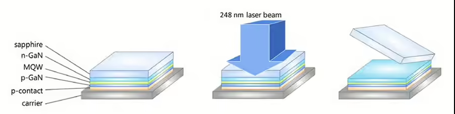
Coherent developed a UV transfer process for the LLO of μLEDs. The LLO process works by irradiating the dies from the rear surface (through the transparent sapphire). This ablates a microscopic layer of GaN, creating a small amount of expanding nitrogen gas that releases the die. The (248 nm) wavelength of our UV transfer process also enables its use with μLEDs grown with some other material variants including AlN. In the UV transfer process, the UV laser beam is reshaped to a rectangular beam with a “top hat” intensity profile before projecting on to the sapphire wafer through a photomask. This uniform intensity ensures identical force is applied at every point within the process field. The optics are configured so that a large area of dies is lifted with each high-energy pulse. This multiplex advantage is unique to our LLO using the UV transfer process based on high energy, UV excimer laser pulses, and will be a critical enabler, supporting reduced costs in high volume production. A similar system from Coherent called UVblade is now widely used in LLO for flex OLEDs.
Excimer-based LLO systems are already in operation in several μLED pilot product lines. Initially motion of the wafer relative to the projected (masked) beam was controlled solely by the encoders on translation stages. “On-Die Processing” is a recent advance and the core of the UV transfer process that now further improves alignment precision, thus enabling smaller dies and narrower streets. “On-Die Processing” also eliminates the possibility of partially illuminating a die on the edge of the laser line. In this case, coarse alignment is still monitored by encoders on the translation stage. But fine alignment is implemented with a closed loop, smart vision system that aligns the wafer relative to the beam using the checker-board pattern of dies. This ensures the edges of the laser field always coincide with the middle of a street and never across a die.
Laser Induced Forward Transfer (LIFT)
The UV transfer transfers and places the selected dies using the principle of Laser Induced Forward Transfer (LIFT), where the challenge is the difference in pitch. On the wafer and the transfer carrier, the dies are closely packed, currently with a pitch of around 1000 dpi. But depending size and resolution, the pitch might be only 50-100 dpi on the display. Plus, the dies must be interleaved, with a red, blue and green die placed in each pixel location.
Existing non-laser transfer methods have been challenged to deliver the necessary throughput at the required resolution. For example, mechanical pick and place methods are limited in speed and placement accuracy, and therefore cannot support the current technology trajectory. On the other hand, flip chip bonders are capable of high accuracy placement (e.g., ±1.5 μm) but can only handle one die at a time. In contrast, UVtransfer can deliver both high (±1.5 μm) accuracy and massive multiplex throughput, moving and placing thousands of dies in a single laser shot.
A benign adhesive strongly absorbs the UV light. The temporary carrier and dies are placed in near contact with the final carrier, which is usually a glass or flex panel already patterned with a TFT backplane and covered with a bonding layer or pads. The UV light is directed from the back of the carrier. Virtually all the laser energy is absorbed by the dynamic release layer that is thereby vaporized. The impulsive force due to the expanding vapor pressure propels the die from the carrier on to the final substrate ideally without residues on the dies.
The LIFT process is being tested with sizes (about 20 µm x 20 µm) and moving forward towards smaller (10 µm x 10 µm) dies. In LIFT, pulses from an Excimer laser enter through the backside of the transparent temporary carrier. The light is absorbed in the buffer GaN layer and vaporizes it. This pushes the LED dies away and onto the display panel substrate, which is placed in close proximity. A final bonding step connects the LEDs to the panel substrate both mechanically and electrically.
The claimed advantages of Excimer LIFT over other mass transfer methods in the fabrication of MicroLED displays include
- High placement accuracy. LIFT can achieve placement precision below 1µm, which is essential for the production of small, high-resolution displays. This level of accuracy ensures that each MicroLED is perfectly aligned, reducing the risk of defective pixels which can compromise display quality.
- Efficiency and speed of LIFT allowing for the transfer of millions of MicroLEDs rapidly and reliably, which is required if manufacturers aim to scale up production without sacrificing quality.
- Flexibility due to the adaptability of laser-based mass transfer to different substrates and MicroLED sizes
As the MicroLED market evolves to utilize even smaller LEDs with tighter pixel pitches, excimer LIFT systems can quickly adapt without extensive retooling or downtime, ensuring that manufacturers can stay ahead in a competitive market.
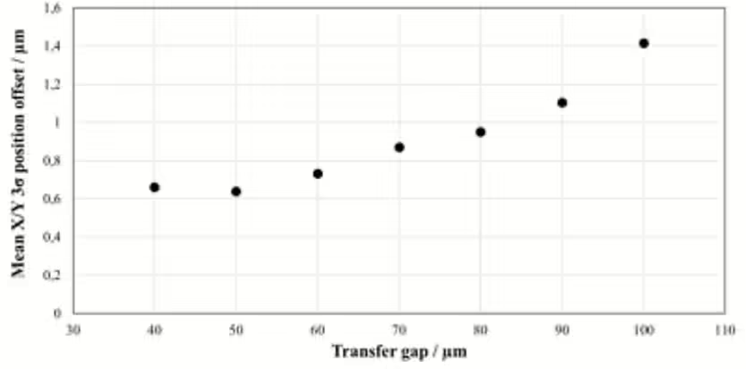
Coherent tested the placement accuracy of LIFT with 5x5x3 µm (thickness) µLEDs as a function of gap distance (distance from the temporary carrier holding the MicroLEDs to the target substrate). The experimental setup used a Coherent UV transfer to move MicroLEDs from a 4-inch GaN donor wafer to a 100 mm diameter quartz recipient wafer. Placement accuracy (in x and y) was measured with a microscope and machine vision system that could automatically identify the dies and determine the center position of each. For each gap distance, 979 MicroLEDs were moved. The graphs show placement accuracy (offset from the ideal position) for all 979 of the MicroLEDs, with a 50 µm gap and die-to-die pitch of 90 µm. To summarize this data, 99.7% (3σ) of the µLEDs were placed within 0.66 µm (x) and 0.56 µm of their of their target location.
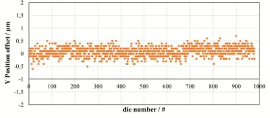
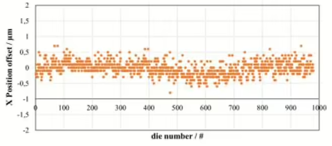
The next graph shows how placement accuracy varied with gap distance. Submicron placement accuracy was maintained at gap distances of up to 80 µm. These numbers show that LIFT is entirely practical with these small MicroLEDs.
Unlike the LLO process, where entire area of adjacent dies are simultaneously processed, the transfer process is the step at which the pitch of the dies is changed from the close separation of the original wafer to the pixel pitch of the final display. This is performed using a photomask with a pattern that only irradiates every 5th die or every 10th die, for example. When the next area of the display is then translated into position for filling with dies, the mask is indexed to move one unit of the wafer pitch, relative to the temporary carrier, enabling a whole new array of dies to be transferred.
Another difference between LLO and transfer is that the latter involves ablation of an adhesive, requiring 5-20x lower laser fluence than a III-V semiconductor. This high efficiency means that high throughput can be achieved with only modest laser powers.
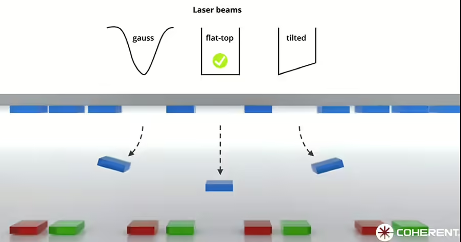
Several other features of UV transfer process are key to its implementation. Even though the gap between the carrier mounted dies and the TFT- substrate is near zero, the impulse force must be managed and controlled in order to achieve successful transfer of every die, with accurate placement and no damage. Specifically, both the magnitude of the force and the direction of the force must be optimized and consistent over the entire display in order to not compromise the process window for the transfer.
Highly uniform and consistent transfer of the dies in the process field demands highly uniform laser irradiation which is a core competency at Coherent that is widely used in diverse applications. This creates a highly uniform 2D field which is then optically reshaped into a square or rectangle with high aspect ratio, in order to match the application. For the transfer of 6” wafers for example, the usable field on the wafer is around 100 mm x 100 mm. As illustrated schematically in the next figure having intensity uniformity on the local (single die) scale means the die is pushed equally across its entire area. Thus, the force is always perpendicular, with none of the lateral shifts that would be induced by a beam with a gaussian or sloped intensity profile. Having a homogeneous beam intensity on the larger (wafer width) scale is equally important, as this ensures that each die is pushed with the same force magnitude.
Repair/Replacement of Rogue Dies
Problem dies are inevitable, so manufacturers can only adopt production technology platforms that are compatible with repair/replacement schemes. Coherent’s UV transfer applied to both LLO, and transfer is compatible with replacement concepts that are already being investigated. The first step in this process is locating and removing bad dies from the wafer. But this then leaves missing spots (that would have been occupied by the removed dies) on the temporary carrier. So, these empty spots must then be refilled on the final substrate. Failed dies can be removed from the wafer before LLO, by applying the process to a selected area only, down to a single die. The map of removed dies from each wafer is then transferred forward and turned into a map of missing dies on the substrate. These can be individually inserted after mass transfer by a similar forward UV transfer process, but this time using a defined single ultraviolet beam. The laser power is matched to whether the laser is ablating a III-V material or a sacrificial adhesive.
Coherent is making great strides in mass transfer and if they can achieve a minimum transfer speed of 250M to 500M die per hour at the required accuracy, yield and cost levels, they will have positioned MicroLEDs to compete in some large display applications. What remains, of course, is getting the die down to under 10µm with cumulative EQEs above 20%. Otherwise the technology will be limited to micro displays used in AR smart glasses, where mass transfer is not required and digital driving minimizes the EQE issues.

Barry Young has been a notable presence in the display world since 1997, when he helped grow DisplaySearch, a research firm that quickly became the go-to source for display market information. As one of the most influential analysts in the flat-panel display industry, Barry continued his impact after the NPD Group acquired DisplaySearch in 2005. He is the managing director of the OLED Association (OLED-A), an industry organization that aims to promote, market, and accelerate the development of OLED technology and products.