Deep ultraviolet (UVC) light technology, particularly in the 210-280nm wavelength range, has been growing in importance for applications like sterilization against viruses and semiconductor manufacturing through photolithography. While traditional mercury-vapor lamps have been the standard for UV photolithography, there’s increasing interest in UV-LED technology as a more efficient, longer-lasting, and environmentally friendly alternative.
A significant challenge in the field has been developing aluminum gallium nitride (AlGaN) deep-ultraviolet MicroLEDs with sufficient power output at small sizes. Smaller MicroLEDs offer higher resolution for applications like maskless photolithography, but traditionally have come with lower light output power. This limitation has been particularly problematic for maskless photolithography, which requires short exposure times but has been hindered by insufficient optical power, leading to protracted exposure times.
The researchers developed advanced fabrication processes to create highly efficient 270nm UVC MicroLEDs in various sizes (ranging from 3μm to 100μm) and built large-format UVC MicroLED displays with high resolution specifically for maskless photolithography.
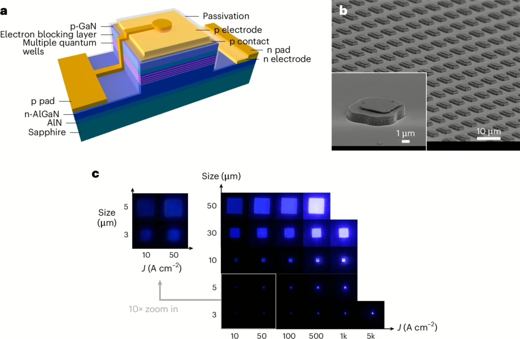
The team employed several innovative approaches. They used a hybrid etching scheme combining inductively coupled plasma and tetramethylammonium hydroxide (TMAH) chemical treatment for precise mesa definition, which enhanced radiative recombination. The researchers applied atomic layer deposition (ALD) to create a 50nm Al₂O₃ passivation layer on the exposed sidewalls to reduce non-radiative recombination centers. They utilized ultrathin annealed Ni/Au metal contacts for the p-contact layer that minimized absorption of UVC light. For larger arrays, they incorporated a highly reflective aluminum-based layer on top of the entire array to enhance front-side light emission. They developed a 320×140 resolution UVC MicroLED display by flip-chip bonding the MicroLED array to a customized CMOS integrated circuit driver.
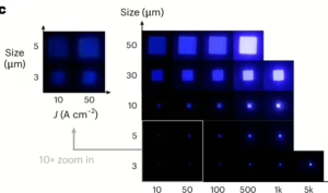
The research yielded several impressive outcomes. The smallest (3μm) device achieved a record-high peak external quantum efficiency (EQE) of 5.7% and a maximum brightness of 396 W/cm². They successfully created 2,540 pixels per inch parallel-connected UVC MicroLED arrays with excellent emission uniformity and light collimation (narrow 48.9° viewing angle). The UVC MicroLEDs and MicroLED displays provided sufficient light power to fully expose photoresist film within seconds, demonstrating practical application for maskless photolithography. Even the smallest 3μm device delivered enough optical power to create patterns on photoresist.
The researchers attribute their success to three key factors: enhanced current spreading uniformity in smaller devices, improved heat dispersion due to higher surface-to-volume ratios, and superior light extraction efficiency. They believe this work opens a path to maskless photolithography that could lead to revolutionary developments in the semiconductor industry by eliminating the need for costly photomasks and significantly reducing manufacturing time and expense.
Reference
Feng, F., Liu, Y., Zhang, K. et al. High-power AlGaN deep-ultraviolet micro-light-emitting diode displays for maskless photolithography. Nat. Photon. 19, 101–108 (2025). https://doi.org/10.1038/s41566-024-01551-7