Modulating the phase of light is part of the means by which holograms are able to create an image. It follows that, to generate a sufficient phase shift, a hologram needs to have a thickness of the order of the wavelength of visible light. This leads to a practical problem.
In order to integrate holograms into physically thin electronic devices, their thickness needs to be reduced to nano meters. Up to now, it has proven difficult to produce such thin holograms in an effective manner. This issue is being addressed by a team led by Min Gu with the Laboratory of Artificial-Intelligence Nanophotonics and CUDOS (Centre for Ultrahigh bandwidth Devices for Optical Systems), School of Science, RMIT University (Melbourne, Australia). Other team members are with the Beijing Engineering Research Centre for Mixed Reality and Advanced Display, School of Optoelectronics, Beijing Institute of Technology (Beijing, China). The team has developed means to create so-called nanometric holograms. The process developed to fabricate the nanometric holograms is represented as both simple and inexpensive.
A recent article published by the team on nanometric hologram technology is entitled “Nanometric holograms based on a topological insulator material.” It was published on May 18 in the journal Nature Communications 8, Article number: 15354 (2017). A copy of the article is available here.
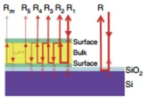
The team’s approach is based on the use of what is called a topological insulator material and that has the formula Sb2Te3. A novel feature exhibited by a thin film of this “quantum material” is that the index of refraction of its surface layers is different from that of its bulk. In the hologram application, a thin film of Sb2Te3 is sandwiched between two semi-transparent metallic surface layers that serve as partial reflectors. In this configuration, an incident light beam can be partially confined within the bulk of the material by multiple reflections between the two surface layers. In effect, the structure acts as a resonant cavity for visible light. This mechanism increases the optical path lengths of the output light beams and, thus, increases the amount of phase shift that is possible. This, in turn, enables realization of a phase-only binary hologram.
The figure below illustrates the configuration and physical mechanism of the Sb2Te3 based thin film cavity.
Diagram illustrating the multiple reflections experienced by light beams within the resonant cavity. The semi-transparent arrows indicate interface reflections.
The technique used to create the computer generated hologram was both simple and fast: ablation by direct laser writing. With laser ablation, the Sb2Te3 thin film was completely removed from designated areas exposing the underlying SiO2 film to air. These areas generate a weak phase modulation due to the small index of refraction of the SiO2 surface. The areas of the Sb2Te3 film not ablated by the laser show a strong phase modulation due to multiple reflections in the optical cavity. Since two levels of phase modulation can be produced, it is possible to generate a binary hologram.
Utilizing the resonant cavity approach, the team produced binary holograms having a thickness of 60 nm and an area of 3 mm x 3 mm.
Holographic images were reconstructed by illuminating the thin film structure with a continuous wave laser beam. The projection angle of the holographic image was designed to avoid overlap between the holographic image and the zero order beam. The laser beam power and its focal position were adjusted to obtain optimal imaging quality.
A video at the end of this article presents a discussion of nanometric hologram technology.
The team investigated several aspects of the creation and performance of the nanometric holograms and report the following.
- The power density of the laser beam affects the hologram morphology and resolution.
- Thicker holograms generate a larger phase shift and thus higher quality holographic images. In addition, the noise level of the image is lower for thicker holograms.
- “Shorter wavelengths produce higher efficiency due to the larger phase shift. However, the light absorption is enhanced in the ultraviolet frequency range, which limits the further improvement of the hologram quality and efficiency. Therefore, to achieve the best holographic image, these parameters need to be balanced.”
In their paper, the team identifies and offer thoughts on aspects of nanometric hologram technology that need to be improved.
First, they conclude that by increasing the thickness and, thus, the extent of the phase modulation, nanometric hologram efficiency can be improved. Second, the efficiency of nanometric holograms can be improved by using highly insulating topological insulator materials with a higher bulk refractive index.
The team went on to state that “The next stage for this research will be developing a rigid thin film that could be laid onto an LCD screen to enable 3D holographic display. They go on to explain that “This involves shrinking our nanometric hologram’s pixel size, making it at least 10 times smaller. Finally, “We are looking to create flexible and elastic thin films that could be used on a whole range of surfaces, opening up the horizons of holographic applications.” -Arthur Berman
RMIT University, Min Gu, [email protected]