In the quest to advance semiconductor technology, researchers have long been exploring new ways to improve the efficiency and scalability of manufacturing processes. Traditionally, the production of semiconductor devices, which power our electronics, involves high temperatures and vacuum conditions, limiting the scale and efficiency of production. A potential game-changer has emerged in the form of solution-processable semiconductors, which offer the possibility of manufacturing under more favorable conditions—such as lower temperatures and ambient pressure—while still delivering high performance. However, a persistent challenge has been the defects that arise in the materials produced through these processes, which degrade device performance.
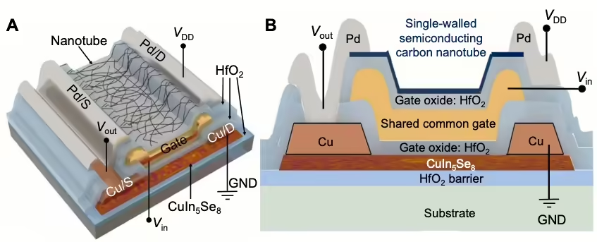
A research team led by Qing Cao at the University of Illinois Urbana-Champaign has made significant strides in overcoming these obstacles. They developed a solution-deposited semiconductor, CuIn5Se8, that remarkably achieves high performance despite containing more defects than its parent compound.
Cao’s lab initially became interested in copper-indium-selenium compounds for their versatility. As Cao explained, “We developed a solution deposition process for these materials, and we experimented with the proportions until we found a material good for electronics purposes, which has a copper-indium-selenium ratio of 1:5:8.” This newly formulated material, CuIn5Se8, surpassed expectations by outperforming both other solution-processable semiconductors and many of the materials currently used in high-performance displays.
One key measure of semiconductor performance is charge mobility, which indicates how easily electrons can move through a material when a voltage is applied. According to Cao’s team, CuIn5Se8 has a charge mobility 500 times greater than the amorphous silicon used in LCD displays and four times higher than the metal oxide semiconductors found in state-of-the-art OLED displays. This is particularly impressive when considering that the material is solution-deposited, which traditionally produces materials with more defects. The mobility of CuIn5Se8 even rivals that of polycrystalline silicon, a material used in smartphone displays, but which requires complex and expensive laser annealing processes to produce.
The researchers’ most surprising discovery came when they investigated why CuIn5Se8 performed so well. “We expected that better-performing materials would have fewer defects,” said Cao, reflecting on their initial assumptions. However, using advanced electron microscopy techniques, they found that CuIn5Se8 actually had more defects than its parent compound, CuInSe2. To resolve this paradox, the team collaborated with theoretical physicist André Schleife, who helped uncover that the defects in CuIn5Se8 were organizing themselves into ordered pairs, a phenomenon that allowed the material to exhibit such high performance despite the defects. These paired defects essentially “cancel out” the negative effects on charge mobility, making CuIn5Se8 a highly effective semiconductor.
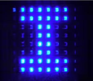
The team demonstrated the material’s potential by using CuIn5Se8 to drive high-performance displays featuring gallium nitride-based MicroLEDs. These LEDs, which are brighter and more durable than the organic LEDs typically used in displays, require powerful transistors to function, particularly at high resolutions. “We demonstrated that our new semiconductor is up to the task,” Cao said, emphasizing that their material not only meets the performance demands but can also be manufactured efficiently using solution deposition.
Looking forward, the applications for CuIn5Se8 extend beyond displays. The material’s ability to form logic circuits that operate at megahertz frequencies opens doors to its use in high-speed electronics, smart packaging, and affordable internet-of-things (IoT) devices. The potential to print high-speed electronics at scale, without sacrificing performance, is particularly exciting for industries like healthcare, where continuous monitoring devices could benefit from such advancements.
Despite the promising results, Cao and his team are proceeding cautiously before pushing for commercialization. Currently, the manufacturing process involves hydrazine, a hazardous chemical often used as rocket fuel. As Cao put it, “It could be used in an industrial setting, but we first want to modify the process to use chemicals that are safer to work with and leave a smaller environmental footprint.”
Reference
Wang, H.-N., An, F., Wong, C. Y., Yin, K., Liu, J., Wang, Y., Zuo, J.-M., Schleife, A., & Cao, Q. (2024). Solution-processable ordered defect compound semiconductors for high-performance electronics. Science Advances, 10(41), eadr8636. https://doi.org/10.1126/sciadv.adr8636