Researchers from Seoul National University (Seoul, Korea) in collaboration with personnel from KAIST (Daejeon, Korea), Samsung Advanced Institute of Technology (Suwon, Korea) and the Korea Photonics Institute (Gwangju, Korea) are developing a new method to deposit microLEDs on sapphire nano-membranes. The new process is reported as having the potential to enable chip singulation without the need for an etching process as well as producing microLED devices with higher efficiency.

To start, a little background information.
The first group of issues that hamper the ability to mass produce microLED displays includes low external quantum efficiency (EQE), high leakage current and a process to transfer the microLEDs onto a display backplane that is both time consuming and costly. The low EQEs and high leakage current have been attributed to plasma etching – a step that is commonly used during device fabrication as part of the chip singulation process. The extent of these problems increases as the size of the microLED devices becomes smaller – and, smaller devices are desired.
The second group of issues that hamper the ability to mass produce microLEDs is due to the lattice mismatch and the difference in thermal expansion coefficients between the LEDs (typically GaN-based) and the substrate (typically made of sapphire). The mismatch induces high defect densities and high compressive stress in GaN layers which, in turn, degrade LED performance.
Recent research by the team was undertaken to address these issues. A just published article on this topic by the team is entitled “A discrete core-shell-like micro-light-emitting diode array grown on sapphire nano-membranes.” The article was published in Scientific Reports, volume 10, Article number: 7506 (2020). A copy of the article is available here.
In the current study, the team adopted an approach in which a 100 nm thick sapphire nano-membrane array was used for the growth of discrete microLEDs each having a size of 4 ?m X 16 ?m. Each microLED was separately grown on an individual sapphire nano-membrane without merging with adjacent ones.
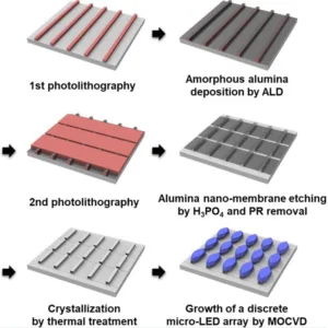
The sequence used in the fabrication of a sapphire nano-membrane array and the subsequent growth of a discrete microLED array is shown in the figure below. “The sapphire nano-membrane array was fabricated by photolithography, atomic layer deposition (ALD) of amorphous alumina, alumina nano-membrane etching for the formation of an array by phosphoric acid (H3PO4) and subsequent crystallization by thermal treatment. During the thermal annealing, the amorphous alumina nano-membrane array was crystallized into single crystalline sapphire (?-phase) by solid phase epitaxy. Then, a microLED array could be separately grown on a sapphire nano-membrane array without the need for a chip singulation process.”
Schematic diagram illustrating the fabrication of a sapphire nano-membrane array and the subsequent growth of a discrete microLED array.
The technical article contains copious details of the equipment and processes used to fabricate the sapphire nano-membrane. The article also includes information on the means used to characterize the microLEDs as well as data on their properties. A few top level comments on the resulting microLEDs include the following:
- The strain in GaN associated with the lattice mismatch between GaN and sapphire substrate was shared with the ultra-thin sapphire nano-membrane. As a consequence, threading dislocation density in the microLEDs was reduced by 59.6% compared to GaN formed on a conventional planar substrate.
- The method improved the internal quantum efficiency of the microLEDs by 44% compared to conventional GaN microLEDs produced on regular planar substrates.
- The microLEDs provided 3.3 times the photoluminescence compared to conventional microLEDs.
- The nano-membranes could be broken using mechanical force. By this means, the microLEDs could be easily separated from the substrate and transferred to the final backplane – without the need for potentially harmful plasma etching.
In conclusion, the researchers stated their hope that this study “will provide a platform technology to realize high efficiency microLEDs by using sapphire nano-membrane, which is suitable for next generation display technology.” In looking towards future work, the researchers explained that the development and fabrication of a vertical type microLED array is currently under way. -Arthur Berman
Euijoon Yoon, Seoul National University, 880-7169, [email protected]