A team or researchers headed by Patricia Jastrzebska-Perfect of the Department of Electrical Engineering and Computer Science at the Massachusetts Institute of Technology are developing a new means to fabricate perovskite-based nanocrystals with precise control over the location and size of each individual nanocrystal. This capability enables the ability to fabricate nanoLEDs which, in turn, opens the potential for their use in applications that include augmented and virtual reality displays.
Integrating halide perovskites materials into micron sized devices is difficult using conventional nanoscale fabrication techniques. More specifically, the difficulty relates to a lack of control over nanoscale patterning. The reasons for this difficulty depends on which conventional approach is utilized. If the approach is based on patterning the perovskite when it is in the form of a fragile thin film and utilizing a conventional lithographic processes, then the required solvents may damage the material. If the approach is based on the use of smaller crystals that are first formed in solution and then picked and placed from solution in the desired pattern, then the problem can be a lack of control, resolution and integration capability.
To overcome these difficulties, the researchers created a technique that allows individual halide perovskite nanocrystals to be grown on-site where needed with precise control over location. Since the material is grown locally with the desired features, conventional lithographic patterning steps are not needed. The technique is also scalable, versatile and compatible with conventional fabrication steps.
A recent article on this topic by the team is entitled “On-site growth of perovskite nanocrystal arrays for integrated nanodevices.” It was published in Nature Communications (2023) 14:3883.
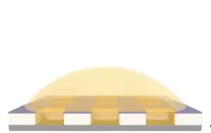
The new process is based on the idea of localizing the solution used in the growth of the nanocrystals. To achieve localization, the researchers created a nanoscale template with small wells to contain the chemical process through which the crystals grown. In addition, the surface of the template and the insides of the wells are controlled for wettability (defined as the ability of a liquid to maintain contact with a solid surface). The purpose of controlling wettability is so that the solution containing the perovskite material does not pool on the template surface but, rather, is confined to the inside of the wells. Having prepared the template, the solution containing halide perovskite growth material is applied to the template and, as the solvent evaporates, the material grows and forms a tiny crystal in each well. The process is illustrated in the figure below which was abstracted from the previously cited article.
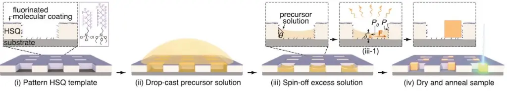
The researchers also found that the shape of the well plays a critical role in controlling the positions in which the nanocrystal grow. This effect occurs because, as the solvent evaporates inside the well, the nanocrystals experience a pressure gradient that creates a directional nano force. The direction of the nano force is determined by the exact shape of the well. As an example of a simple case, when the wells are square, the crystals have an equal chance of being placed in each of the well’s four corners. It was also found that changing the size of the wells controlled the amount of growth solution inside the well and this, in turn, controlled the size of the crystals.
The researchers demonstrated the effectiveness of this new technique by fabricating precise arrays of nanoLEDs. Utilizing this new technique, the researchers formed patterned arrays of CsPbBr3 nanocrystals with tunable dimensions down to less than 50 nm and positional accuracy less than 50 nm. The nanoLEDs acted as nanopixel and emitted light when electrically activated.
In the future, the researchers plan experiments to determine how small devices can be made utilizing the new technique.
Reference
Jastrzebska-Perfect, P., Zhu, W., Saravanapavanantham, M. et al. On-site growth of perovskite nanocrystal arrays for integrated nanodevices. Nat Commun 14, 3883 (2023). https://doi.org/10.1038/s41467-023-39488-0