Frank (Qun) Yan, Professor at Fuzhou University (China) & General Manager of SID China gave the first microLED talk titled MicroLED driving the third wave of technology revolution of information display. This talk was an introduction to microLEDs and all of his important points have been incorporated above.
Jihoon Kang from Samsung Electronics was the second speaker and he talked about Micro LEDs for TV applications: Technical Challenges. His talk was also mostly introductory and all his important points have already been discussed.
François Henley was representing both Tesoro Scientific and QMAT, Inc in his talk titled Enabling Laser-based Mass Transfer of LEDs at Over 100M Devices per hour. His talk was more technical and focused on two key issues with microLED displays:
- How to inspect the epitaxial wafer to ensure only good LEDs were transferred from the wafer to the backplane. (Tesoro Scientific)
- How lasers can be used to transfer die at very high rates and only transfer the die known to be good from the initial inspection. (QMAT, Inc)
Henley started with a discussion of yield in microLED display systems. This portion of the talk was utterly convincing – the microLED wafers must be tested and microLEDs that test bad must not be transferred to the display backplane.
Testing microLEDs is not, however, simple. One way of testing chips on a wafer is mechanical probing of the wafer, a process used on systems like microprocessors. With the very small die and the very large number of die on a wafer, this process is not practical for microLEDs. Besides, in flip-chip microLED designs, the points that need to be probed may not be accessible.
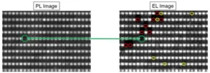
He compared two testing methods he called PL (Photoluminescent) and EL (electroluminescent). Both of these methods illuminate the entire wafer with light of a chosen wavelength and then a high resolution camera examines the wafer to see which die light up. In the PL system, the wavelength of the light is chosen to excite the III-V material, which then emits its characteristic wavelength, much like illuminating a QD with blue light and seeing it glow. According to Henley, this tests the epitaxial material but microLEDs can be made from the correct material and still not have acceptable properties.
In the EL system, the light serves to generate electric currents in the wafer. These currents then excite the microLEDs and they emit light much like they would if driven electrically. One or more test enhancement layers needs to be incorporated in the epitaxial substrate for the EL process to work.
Comparison of the PL and EL images for a microLED wafer. (Source F. Henley at ADS)
Tesoro Scientific makes a wafer inspection system that performs both of these tests and records the positions of bad microLEDs. This data is then available to the mass transfer system so the system does not transfer bad die to the display substrate. The system is said to have a very low false-positive rate. This is important because if the system evaluates a microLED as good and if it really is bad, the mass transfer system will then transfer the die to the display substrate. When the display is finished and tested, the bad die is then discovered. It must be removed and replaced by a good die in a time consuming and expensive repair process. A false negative, one that identifies a good microLED as bad, is far less costly – that microLED is just not used, increasing epi cost for the display slightly.
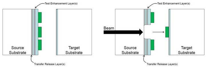 Laser-based mass transfer system (Source: F. Henley at ADS)
QMAT, Inc is in the process of developing a laser-based mass transfer system that can be driven by the known good die (KND) data file from the PL/EL inspection system (or, presumably, by any other inspection system.) When a system like this is used, in addition to the test enhancement layer, the epi substrate must have a transfer release layer. When a laser pulse hits this transfer layer, it “blasts” the die across the very small gap onto the target substrate without affecting the adjacent die.
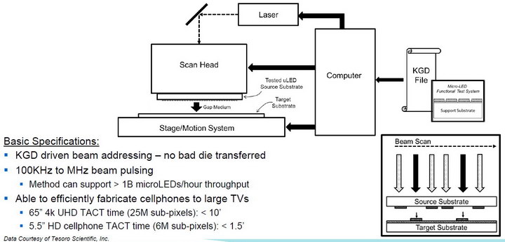 Layout of a complete laser mass transport system. (Source: F. Henley at ADS)
In a system like this, one die is transferred at a time. However, the laser can be pulsed at speeds from 100KHz to 1MHz and the system is said to be able to transfer more than 1 billion die per hour. This would mean a 55” 4K TV would take about 10 minutes to make while a 5.5” cellphone display with FHD resolution would take about 1.5 minutes.
The insert in this image shows that every die is not transferred on every laser scan. If the die spacing on the target substrate is to be 3x the die spacing, every third die is transferred on a given scan. If the target die spacing is 20x the epitaxial die spacing, only every 20th die is transferred on a given scan. The other 2 or 19 die are transferred on a later scan, after the motion stage has moved the target substrate to a new position. Motion between die transfer laser scans is typically on the order of the die spacing on the target substrate.
Clearly, this system needs extreme precision in the substrate motion stage, the laser beam scanning system and the laser pulse timing system. This should be expected – transferring 25M of anything to anywhere with 1µm or so accuracy is going to require extreme precision.
Falcon Liu from PlayNitride talked about MicroLED Display — the Next Generation Display Technology.
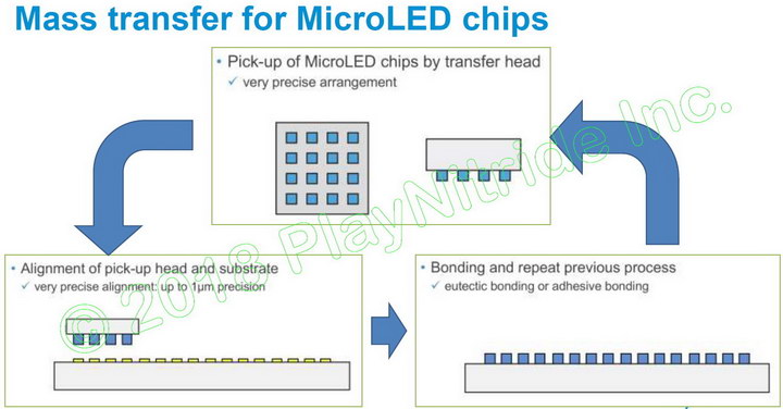 Mass transfer of microLEDs by PlayNitride (Source F. Liu at ADS)
This talk was mostly a background and review talk and did not give sufficient information to evaluate or even understand the mass transfer process being developed by PlayNitride.
![]() PlayNitride’s 128 x 128 PixeLED Display was demonstrated at the ADS (Credit: M. Brennesholtz)
PlayNitride’s 128 x 128 PixeLED Display was demonstrated at the ADS (Credit: M. Brennesholtz)
In the exhibit room at the ADS, PlayNitride was demonstrating its 128 x 128 PixeLED. This was on a transparent substrate and had a 50% transmission. The display was 2.65″ square with a sub-pixel resolution of 68ppi, said to be about what is needed for a 65″ 4K TV.
Prof. Yong Sang Kim from SungKyunKwan University in Seoul, Korea gave a talk titled Backplane Technologies for Micro-LED Display. This talk, as expected, focused on the backplane design and driving schemes for microLED displays. These schemes include both active and passive matrix designs and both amplitude and pulse modulation of the individual microLEDs.
One of the key problems with a silicon backplane for a microLED microdisplay is the thermal expansion differential between silicon and III-V LED materials. This thermal expansion problem can cause problems and lead to failure of the microdisplays. He discussed some of the schemes used by some of the companies using monolithic and hybrid to minimize this problem.
Fang Ou from Hong Kong Beida Jade Bird Display (JBD) Ltd gave a talk titled Wafer-Level Monolithic Hybrid Integration: a mass manufacturable approach towards high performance microLED micro-Displays.
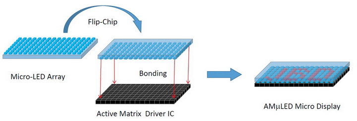 Overview of the JBD flip-chip design. (Source, Fang Ou at ADS)
JBD is focusing on microdisplays and uses a flip-chip approach to making these displays, as shown in the image. The company says it is capable of making microLEDs with sizes ranging from 2µm – 10µm that will have center-to-center spacing from 3µm – 20µm.
JBD is also developing a process where a blank epi wafer is bonded to the active matrix wafer. The microLEDs are then formed in this epi wafer using standard semiconductor processing steps. The advantage of this approach is since there are no microLEDs on the epi wafer before bonding, just uniform epitaxial material, the alignment between the epi wafer and the backplane wafer need not be nearly as precise as it would be if the microLEDs had already been formed.
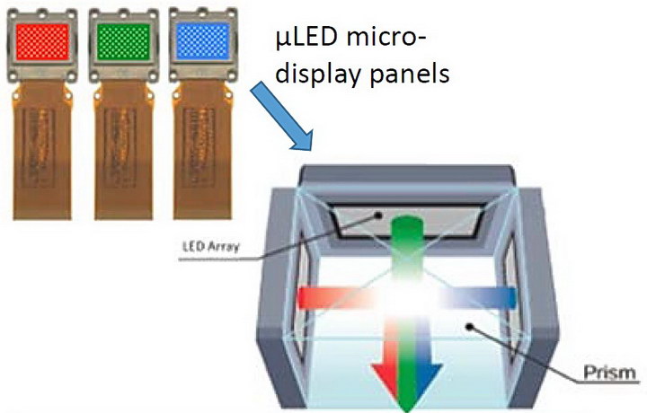 MicroLED microdisplay light engine from JBD (Source: Fang Ou at ADS)
One of the problems with microdisplay-based microLED systems is that, to date, all microLED microdisplays are monochrome and very few modern non-military applications want monochrome images. To overcome this problem, JBD uses a color-combining X-prism, similar to the ones used in a 3LCD projector. They say this takes up no more room than a DLP or LCoS projector used in an AR HMD because those systems have TIR and PBS prisms in the system and these prisms take up just as much space as an X-prism.
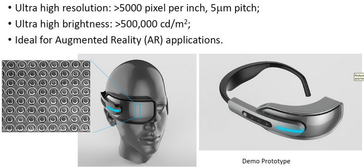 JBD’s AR HMD Prototype (Source: Fang Ou at ADS)
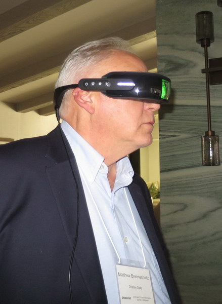 Meko’s Matt Brennesholtz tests the JDB AR HMD prototype at the ADS (Credit: M. Brennesholtz)
JBD has built a prototype full color AR HMD based on its red, green and blue microLED microdisplays. They brought this unit, which has a 2560 x 1920 resolution, to the ADS and I got a chance to test it. While I was told only about 5% of the light from the microLEDs made it to the eye, the system was still very bright. It also produced a lot of stray light, as can be seen coming out the front of the see-through HMD in the image. Between the stray light, the extremely bright AR image and the moderate light levels in the demonstration room, it was hard to evaluate the see-through properties of the system although it was definitely see-through.
JBD seems to be on the right track for the development of AR systems that will be usable in high ambient light environments. They were also demonstrating individual red, green and blue microdisplays and had a neutral density filter that reduced the light level about 1000x on hand to allow examination of these displays, especially the green display, without burning out your eyeballs.
Vincent Lee, Founder and CEO of Lumiode and a friend of mine from the SID-MAC chapter gave a talk titled High-Brightness Micro-LED Microdisplays by direct integration of LEDs and Silicon Thin-Film Transistors. Lumiode makes microLED microdisplays by taking the microLED epi wafer and depositing a layer of amorphous silicon on it. Laser recrystallization is then used to convert this to polysilicon. Then standard semiconductor processes can be used to create the TFT drive circuitry.
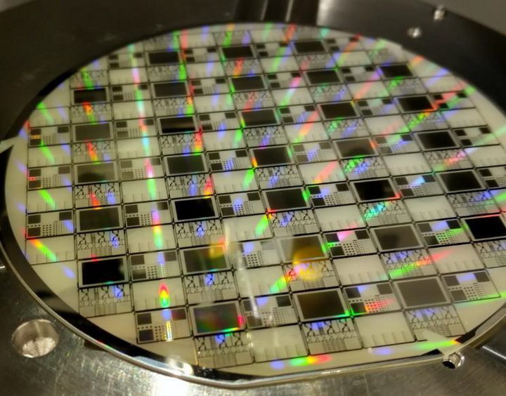 A microdisplay wafer from Lumiode. (Source: Vincent Lee at ADS.
Lee says this process is capable of producing green microdisplays with up to 10,000,000 cd/m² (nits). He says the process is LED epi technology agnostic and is capable of producing any color of microdisplay. He added that this process decouples External Quantum Efficiency (EQE) from microLED size and showed data that the EQE was about 20% for die sizes from 5µm to 80µm on a side.
The final presentation on microLEDs and the last presentation at the ADS was from Boris Kobrin of N-Tech Research and was titled Mass transfer technology – a key for LED cinemas commercialization. This was another (but still very useful) talk that provided a lot of the information use at the beginning of this article, including all of the forecasts. – Matthew Brennesholt