Researchers at Korea University (KU) and the Samsung Advanced Institute of Technology (SAIT) have developed a new type of thin film transistor (TFT), which is much faster than its predecessors. The development has been called ‘an important step toward speeding up image display on devices like TVs and smartphone screens’.
The new TFT was made from zinc oxynitride (ZnON), which was then plasma treated with argon gas.
In the past, work using zinc oxide materials focused on the addition of metal cation, such as indium with gallium, hafnium, zirconium and lanthanide. Used in semiconductors, these materials have electron mobility values of between 5 and 20 centimetres squared per voltsecond. Under ideal lab conditions, higher speeds (such as graphene’s 200,000 cm²/vs) have been recorded; however, TFT speeds in commercial electronics are usually in the single- to double digit range.
Sanghun Jeon, associate professor at KU, said, “For future electronic devices, the mobility of the active oxide channel materials needs to be further increased above 100 centimeters squared per voltseconds”. The ZnON transistor built by Jeon’s group, and their colleagues at SAIT, has speeds ‘about 10 times greater’ than their previous devices.
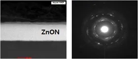
Cross-sectional high angle annular dark field scanning transmission electron microscopy image and nanobeam diffraction pattern of Ar plasma treated ZnON Active oxide semiconductors, such as the ZnON device, benefit from low production costs and a relatively low fabrication temperature (below 300°). This makes them ‘easy’ to integrate with various organic and inorganic materials.
As a thin film, ZnON exhibits fast mobility rates, due to its ability to deactivate oxygen vacancies. These are defects in transition metal oxide surfaces, which occur due to unavoidable bonding flaws in creating the compound.
When the negatively-charged oxygen ion (anion) in ZnO is substituted with a nitrogen anion, the valence band (highest range of electron energies in which electrons are normally present at absolute zero) edge of ZnON is positioned above the previous location of the neutral oxygen vacancy in ZnO. This effectively buries the vacancy below the valence band edge, and prevents gaps in conductance.
The ZnON thin films were constructed by sputtering a mix of N2, O2 and argon gases through a rotating holder onto a zinc target. The O2 partial pressure in the chamber was varied during the deposition by adjusting its flow rate; the nitrogen and argon rates were kept constant. This was done to control the anion contents of the films. The result was a glassy, composite film around 50nm thick, which was relatively unstable due to nitrogen’s low reactivity with zinc relative to the atmospheric oxygen.
The argon plasma process mentioned above was adopted to combat this instability. In the process, a film is bombarded with the high-energy plasma form of argon. This caused cascades of atomic and ionic collisions and energy dissipation inside the material. These cascades reordered the bonds between the zinc, oxygen and nitrogen atoms into a chemically uniform nanocrystalline structure, in an amorphous matrix. This improved the material’s stability under radiation and electrical stress.
When compared to a film that had not been plasma treated, the new film showed no evidence of nitrogen loss through diffusion, after both were exposed to atmospheric conditions for 30 days.
Under conductance tests, the channel mobility of the nanocrystalline TFT was found to be 138 cm²/vs.
Future work includes incorporating other metal cations in their metal oxynitrides. They also intend to examine the effects of plasma and vacuum UV exposure on the films.
Analyst Comment
This is an interesting development. It brings mobility that is much better than a-Si, without the instability that some oxides have hit and without the costs of LTPS. (BR)