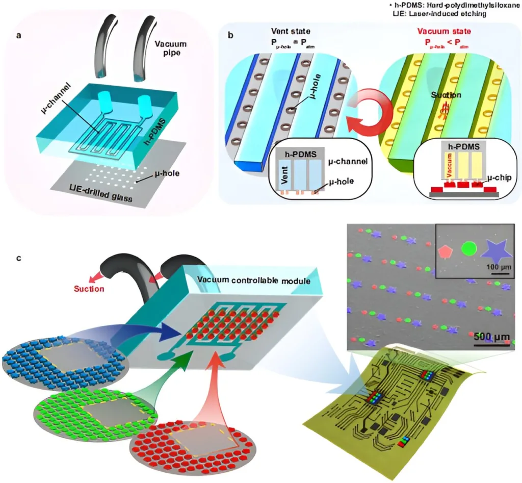
Researchers at the Korea Advanced Institute of Science and Technology (KAIST) are reporting a new method of transfer printing for inorganic thin-film semiconductors, addressing challenges in the field of soft electronics. This method, known as Micro-Vacuum Assisted Selective Transfer (μVAST), involves creating micro-hole arrays on a glass substrate using a laser-induced etching technique. The process allows for the selective transfer of semiconductor microchips onto various substrates, including flexible ones, without requiring additional adhesives or causing damage to the chips.

The μVAST technique relies on a vacuum-controllable module (VCM) composed of micro-channels and laser-drilled holes to generate a micro-vacuum force for picking up and placing semiconductor chips. It offers higher adhesion switchability, precise control, and reduces the risk of damage to the chips compared to traditional transfer methods. This makes it suitable for assembling micro-sized inorganic semiconductors on unconventional substrates.
Professor Keon Jae Lee, who lead the research teams, says, “The micro-vacuum assisted transfer provides an interesting tool for large-scale, selective integration of microscale high-performance inorganic semiconductors. Currently, we are investigating the transfer printing of commercial microLED chips with an ejector system for commercializing next-generation displays (Large screen TVs, flexible/stretchable devices) and wearable phototherapy patches.”
The method has been demonstrated to be effective for transferring various semiconductor materials, including flexible MicroLEDs and silicon transistors, onto different substrates. μVAST seems to show high transfer yield and repeatability, which are crucial for commercial applications in electronics manufacturing.
Flexible Electronics
Flexible electronics and displays are an emerging field enabled by advancements in materials and manufacturing. They have potential applications in wearables, skin electronics, curved screens, etc. However, fabrication limitations have hindered commercialization.
MicroLEDs are an extremely promising candidate for next-gen displays due to performance advantages over other technologies. But they come with sky-high costs from complex transfer printing processes to integrate the LEDs onto final substrates. Mass transfer techniques that are scalable yet precise are critical to slash prices.
Various transfer techniques exist – stamping, laser assist, fluidic assembly, etc. – but still face issues like low selectivity, chip damage, poor yields, etc. Micro-vacuum force has been utilized too, but better selective control is needed for reliable, cost-effective transfer.
Micro-hole drilling of glass can enable novel microsystems, but conventional methods like etching and laser drilling have limitations around precision, aspect ratios, cracks, etc at the microscale. However, an advanced technique called laser-induced etching (LIE) offers promise for high-speed drilling of complex 3D micro-hole arrays.
The researchers leveraged LIE micro-holes and vacuum control modules to develop a novel selective transfer approach dubbed μVAST. It achieves greatly enhanced switchable adhesion and selectivity for mass transfer printing vs. existing options. Heterogeneous integration onto diverse surfaces is enabled with high yields and no extra adhesives.
Reference
Park, S. H., Kim, T. J., Lee, H. E., Ma, B. S., Song, M., Kim, M. S., Shin, J. H., Lee, S. H., Lee, J. H., Kim, Y. B., Nam, K. Y., Park, H.-J., Kim, T.-S., & Lee, K. J. (2023). Universal selective transfer printing via micro-vacuum force. Nature Communications, 14(1), 7744. https://doi.org/10.1038/s41467-023-43342-8

