Researchers are proposing a novel approach to creating high-resolution organic semiconductor patterns, which are crucial for developing advanced microelectronics and optoelectronics, particularly for wearable technologies.
In the traditional process, a uniform thin film of organic semiconductor material is first deposited across the entire substrate surface. This method is straightforward but can be inefficient and result in material wastage because only specific areas of the film will be used in the final device structure.
Once the film is deposited, photolithography or another patterning technique is employed to define the desired structures. This involves coating the film with a photoresist, exposing it to UV light through a mask to define patterns, and then using chemical etching to remove unwanted areas. However, this approach can damage sensitive organic materials due to exposure to UV light, heat, or chemicals during the patterning process.
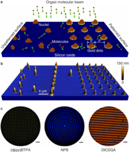
In the researchers’ new method, the strategy is to invert the traditional film growth and surface patterning method to surface patterning and patterned growth. This involves initially patterning the substrate surface and then depositing organic semiconductor molecules, allowing them to diffuse and selectively nucleate at designated areas. This technique enables high-resolution patterning of organic materials and the creation of ultra-high resolution microelectronic and optoelectronic device arrays. It also allows for hetero-patterning, physical property tuning, and anisotropic growth on surfaces by manipulating molecule-template-substrate interactions, hierarchical templates, and growth parameters

The experimental results and theoretical simulations demonstrated that the patterned growth technique was highly effective, achieving a pattern yield of up to 100% when using mechanisms based on binding energy differences and step-edge-induced growth. In these methods, the organic molecules preferentially nucleated and grew on areas of the substrate where the binding energy was higher or along step edges, leading to nearly perfect pattern formation. These areas serve as nucleation centers, ensuring that the organic molecules deposit precisely where intended. However, when the surface molecular density modulation mechanism was employed, the yield was slightly lower, at 95%. This method relies on variations in the local concentration of molecules on the substrate to guide nucleation. Although highly effective, it is slightly less precise than the other two mechanisms due to the inherent variability in molecular diffusion and aggregation on the substrate, which can lead to occasional deviations from the intended pattern.
OLEDs benefit from this technique as it enables the creation of ultra-high-resolution patterns essential for improving display quality and efficiency. In wearable electronics, where flexibility, lightweight, and low power consumption are critical, this method allows for the fabrication of components that meet these requirements without the damage associated with traditional patterning processes. The research creates new potential for integrating OLED into compact, flexible, and energy-efficient wearable devices.
References
Wang, W., & Chi, L. (2024). Patterned growth of organic semiconductors for ultra-high resolution microelectronics and optoelectronics. Wearable Electronics, 1, 91–110. https://doi.org/10.1016/j.wees.2024.05.005