Metal halide perovskites have garnered significant interest as promising materials for next-generation optoelectronic devices due to their outstanding optoelectronic properties. Researchers have made rapid strides in device performance by gaining a profound understanding of perovskite composition, crystal growth, and defect engineering. However, to achieve higher efficiency as device performance approaches theoretical limits, effective optical management is becoming increasingly crucial.
Korea’s Chungnam National University’s Professor Seong-Min Kang and Sungkyunkwan University’s Professor Jin-Wook Lee have collaborated on new review, published in Nano-Micro Letters, to explore the latest research trends and results in multi-scale patterning technology for optimizing perovskite optoelectronic devices.This review emphasizes the significance of efficient light harvesting and light outcoupling in perovskite optoelectronic devices. These devices are designed to mutually convert light energy and electrical signals through a specific compound structure known as perovskite. To achieve this, it is essential to efficiently absorb light energy (light harvesting) and efficiently emit light through electrical energy (light outcoupling).
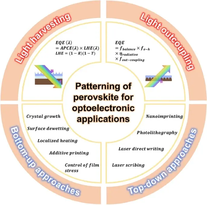
To address the challenges related to optical management, the research team focused on multi-scale patterning technology. This involves forming nano/micro composite structures in perovskite optoelectronic devices. By implementing this approach, the team aimed to enhance the photoelectric conversion efficiency of these devices significantly.
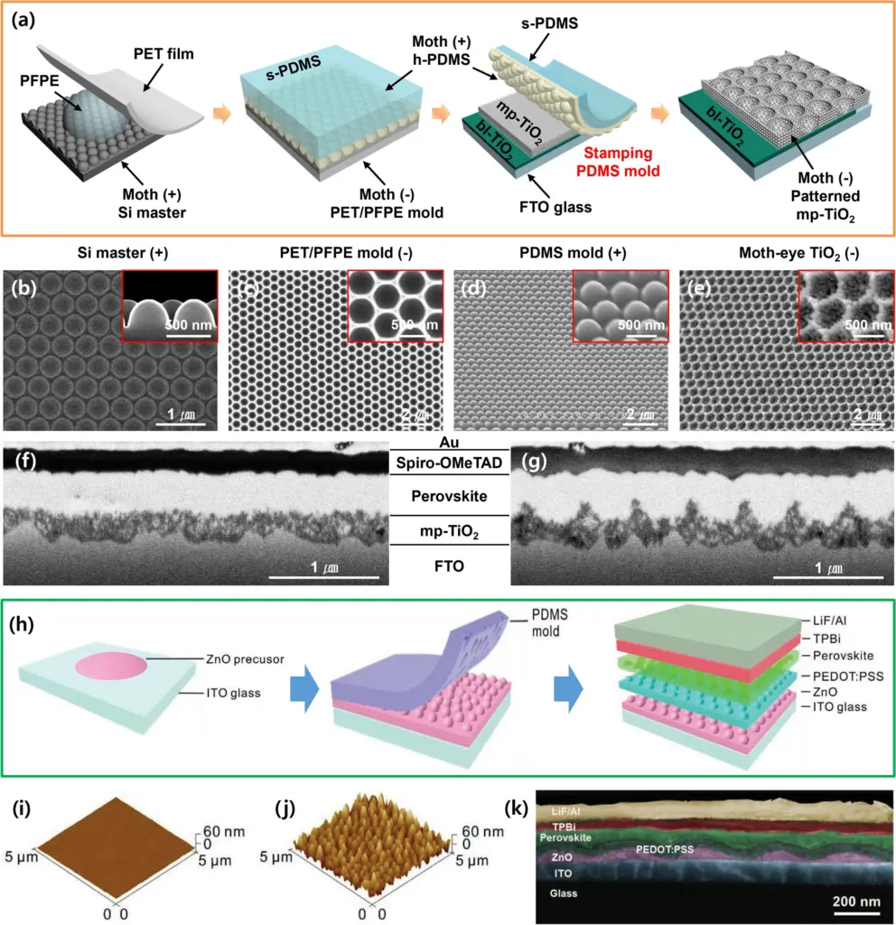
In the top-down approaches, various methods like nanoimprinting with PDMS molds, photolithography, and laser-assisted techniques are used to create nanopatterns on perovskite layers, leading to improved light harvesting efficiency (LHE) and light outcoupling efficiency. However, these methods face challenges related to precision, damage to the perovskite layer, and limited resolution. On the other hand, bottom-up approaches involve controlling perovskite crystal growth at the atomic or molecular level, employing techniques such as surface dewetting, localized heating, additive printing, and film stress control. While these methods offer advantages, they suffer from complex procedures, low process speed, and poor film uniformity.
To address the limitations and enhance perovskite device performance, several suggestions are put forward:
- Hybrid methods combining top-down structuring and bottom-up crystal growth could yield more controllable nanopatterns with improved durability and stability.
- Enhancing light harvesting and outcoupling abilities through nanopatterning transparent electrodes or using nanoparticles in anti-reflective layers can increase the efficiency of perovskite solar cells and light-emitting devices.
- Electrospinning/spraying perovskite fibers is proposed as a viable option for flexible and large-scale 3D perovskite applications, while exploring chemically stable polymers as alternatives to PDMS molds is suggested.
Regarding encapsulation, patterned polymer films with liquid repellent properties are viewed as potential alternatives to traditional cover glass methods, offering added flexibility, stretchability, and reusability for perovskite devices.
The study presents an extensive guideline for incorporating existing multi-scale patterning technologies to improve the photoelectric conversion efficiency of perovskite devices. It offers promising prospects for future research and development in the field of energy convergence technologies, potentially benefiting perovskite solar cells, LEDs, and optical sensors.
Reference
Lee, JW., Kang, S.M. Patterning of Metal Halide Perovskite Thin Films and Functional Layers for Optoelectronic Applications. Nano-Micro Lett. 15, 184 (2023). https://doi.org/10.1007/s40820-023-01154-x