MIT researchers have successfully developed a scalable technique that allows for the precise integration of halide perovskite nanocrystals in nanoscale devices, overcoming the challenges associated with conventional fabrication and patterning techniques. The breakthrough holds great potential for various applications, including on-chip light sources, photodetectors, and memristors.
Halide perovskites have garnered significant attention due to their exceptional optoelectronic properties and potential applications in high-performance solar cells, light-emitting diodes (LEDs), and lasers. However, integrating these materials at the nanoscale has proven difficult, as they are delicate and can be damaged during conventional fabrication processes.
The MIT researchers devised a novel approach to grow individual halide perovskite nanocrystals on-site with precise control over their location, accurate to within less than 50 nanometers. The technique also enables precise control over the size of the nanocrystals, which is crucial as size directly affects their characteristics. By growing the material locally without the need for conventional lithographic patterning steps, which can introduce damage, the researchers achieved a significant breakthrough.
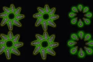
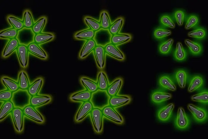
Furthermore, the technique is scalable, versatile, and compatible with conventional fabrication steps, allowing for the integration of nanocrystals into functional nanoscale devices. The researchers utilized this method to fabricate arrays of nanoscale light-emitting diodes (nanoLEDs), which are tiny crystals capable of emitting light when electrically activated. Such arrays have immense potential in applications such as optical communication and computing, lensless microscopes, quantum light sources, and high-density, high-resolution displays for augmented and virtual reality.
The researchers created nanoscale templates with small wells that contain the chemical process through which crystals grow. By modifying the surface of the template and the wells’ interiors, they controlled the wettability property, ensuring that the perovskite material remains confined within the wells and does not pool on the template surface.
Applying a solution containing halide perovskite growth material to the template, the researchers observed the formation of tiny crystals within each well as the solvent evaporated. They discovered that the shape of the wells played a critical role in controlling the nanocrystal positioning. By altering the well’s shape, they manipulated nanoscale forces, resulting in preferential placement of the crystals in the desired location.
Additionally, the size of the crystal formed inside each well could be controlled by adjusting the well’s size to allow more or less growth solution. This tunability allowed the researchers to fabricate precise arrays of nanoLEDs, wherein each nanocrystal served as a nanopixel emitting light. These high-density nanoLED arrays have significant potential in various applications, including on-chip optical communication and computing, quantum light sources, microscopy, and high-resolution displays for augmented and virtual reality.
Moving forward, the MIT researchers plan to explore additional applications for these nanoscale light sources, further test the limits of device miniaturization, and effectively incorporate them into quantum systems. Moreover, the developed technique opens up opportunities for developing halide perovskite-based on-chip nanodevices. Additionally, it provides a convenient means for researchers to study materials at the individual nanocrystal level, facilitating further investigations into these unique materials and inspiring diverse applications.
This groundbreaking research was supported in part by the National Science Foundation and the MIT Center for Quantum Engineering.
Research
Jastrzebska-Perfect, P., Zhu, W., Saravanapavanantham, M. et al. On-site growth of perovskite nanocrystal arrays for integrated nanodevices. Nat Commun 14, 3883 (2023). https://doi.org/10.1038/s41467-023-39488-0