MicroLED display technology is making steady progress towards commercialization. The technology still faces several complex manufacturing challenges, which will take time to resolve. Display Week 2021, gave a glimpse of microLED technology developments by various companies to resolve the manufacturing issues.

MicroLED has the potential to outperform both LCD and OLED technologies in terms of color reproducibility, brightness, reliability and low power consumption. To compete with LCD (Quantum Dot & miniLED) and OLED in the consumer market, microLED products need to have zero defects, high performance, high uniformity, high volume scalability and cost competitive manufacturing. The success of commercialization and mass production will depend on the ability to scale up for volume production with competitive price performance.
Increasing Investments
According to Yole’s presentation at DisplayWeek 2021,
“more than 8900 MicroLED display patents have been already filed by 480 organizations. More than $5.1 Billion has already been spent on MicroLED. Start-ups raised more than $250 million in the last 18 months. Display makers dominate activity followed by start-ups. Chinese companies have been dominating activity (45%) and Korea came back strongly in 2020 (22%) driven by Samsung and LG. Samsung was most active in 2020, followed by CSOT, BOE, Visionox, Playnitride, Konka and Facebook. More than 50 prototypes of products have already been produced by more than 30 companies. Samsung has introduced a 4K 110-inch MicroLED TV (2021) but it costs $155K. Vuzix promised to ship the first AR device based on JBD (Jade Bird Display) MicroLED later this year”.
Complex Manufacturing
MicroLED is a self-emitting display consisting of arrays of microscopic LEDs each forming a pixel. It has a simple structure but a complex manufacturing process. The microLED supply chain consists of the following steps.
- GaN epiwafer LED creation
- Processing of thin film LEDs
- Mass transfer of the chips to the display backplane
- Inspection and repair processes
Display integration of MicroLED can be heterogeneous or monolithic integration. In the heterogeneous type, makers use pick and place process to make microLED arrays, and chips are transferred from an epiwafer or carriers to the display backplane (LTPS or Oxide TFT on a glass or flexible PI substrate). The monolithic integration process involves microLED array and backplane hybridization.
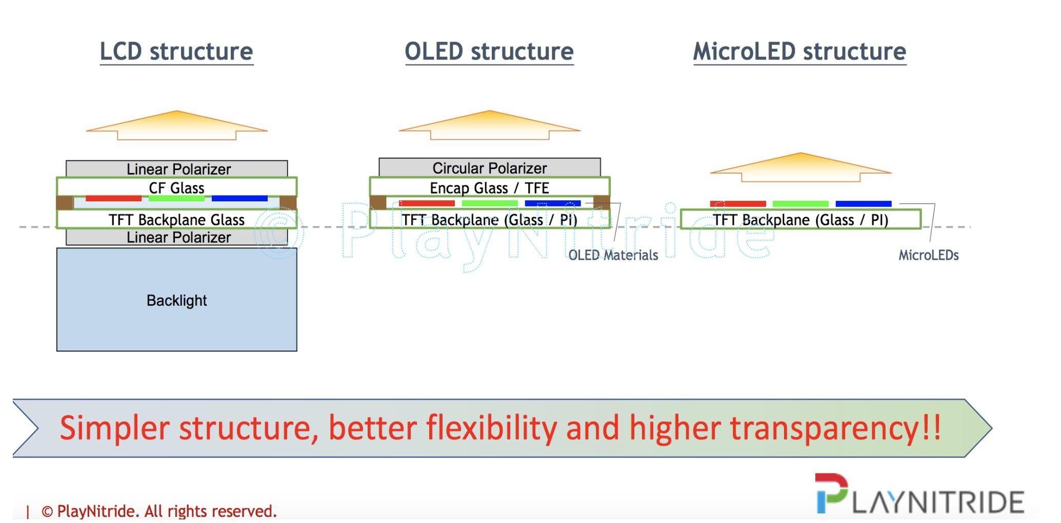 Source; Playnitride DisplayWeek 2021
Chip Manufacturing
Companies are developing solutions to reduce costs and remove roadblocks for MicroLED commercialization. Saphlux has developed NPQD technology that integrates an RGB pixel within one chip. This process can reduce total system costs. According to DSCC’s microLED presentation, at Display Week 2021,
“Triad chip (RGB sub-pixels built into a single chip)(offered by Seoul Viosys),
- Pros: (a) reduced cost of mass transfer (b) larger chips: easier to handle during transfer/ repair.
- Cons: (a) with native colors: increase complexity and cost of the LED manufacturing (b) with color convertors: QD material costs.
Smartpixel (microLED bonded on Microdriver IC)
- Pros: removes the need for TFT backplane
- Cons: cost of CMOS wafer and hybridization”.
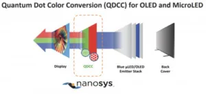
Color Conversion: The mass transfer process that requires bonding RGB (Red Green Blue) MicroLED to the display backplane accurately and efficiently is very challenging. Also different colors of LED need slightly different voltage and drive currents. Color conversion by Quantum Dots (QDs) (QDCC) or by phosphor provides another alternative. Using single-color (blue) MicroLED chips and color converting them with QD layers can help in the manufacturing process.
Nanosys’s presentation at DisplayWeek 2021 showed
“a breakthrough of new heavy metal free green QDCC emitter that delivers product ready brightness, color accuracy and reliability. The microLED size needs to be below 7 micron to be cost competitive in future displays.”
According to the company its color-converted red provides 3.5x better performance at an economical cost, and is crucial for emerging display applications. AR requires ultrahigh efficiency and brightness. QDCC microLEDs at 1.8 microns can deliver the resolution and energy efficiency required for the future of AR.
Nanosys has acquired the microLED display company “gl?” recently to accelerate MicroLED development & adoption.
 Figure: 2 Source:Nanosys
Inspection, Repair & Yield
Manufacturing and yield problems can become issue in epitaxy, chip, mass transfer, bonding, driving technology, backplane, inspection and repair. The integration of in-process test, redundancy and repair are used to improve yield. Also as display resolutions gets higher, pixels are getting smaller: the trend is moving from 50 micron to 5 micron to 1 micron. This requires development of inspection tools that can achieve sub-micron resolutions. According to an InZiv presentation, it has built high-resolution inspection tools that can inspect any size microLED and analyze defects to improve processes and accelerate time to market. InZiv makes high-resolution tools for OLED and QLED also.
MicroLED companies also need to use mass testing and repair methods to reduce the cost and time of assembly. Companies such as Toray are working on equipment for microLED wafer inspection, repair and transfer. Laser repair equipment can remove defective microLEDs. As a presentation by DSCC on microLED session explained
“redundancy is an alternative way to reduce number of defective pixels. However, redundancy is expensive as it greatly increases LED consumption and the number of transfers. If the speed of the repair process is high enough, redundancy should not be required.“
Uniformity: microLED chips need wavelength uniformity and thickness uniformity for display applications. Solutions from MOCVD suppliers such as Aixtron, Veeco and others are helping to resolve issues caused be poorer uniformity. According to an Instrument Systems (Konica Minolta Group) presentation, the uniformity analysis of displays requires accurate color and luminance measurements. A combination of a highly accurate spectroradiometer and a fast RGB camera can provide a fast and accurate solution.
There’s a lot happening in MicroLED so I’ll cover issues of mass transfer, the challenge of supply development and applications in Part 2. (SD)
We’ll be publishing part 2 shortly after Part 1 so, to continue reading, you can link here (MicroLED Display: Road to Commercialization (Part 2))
Publisher’s Note (the two parts of this article will be counted as a single one for the purposes of your free article allowance)
Sweta Dash is the founding president of Dash-Insights, a market research and consulting company specializing in the display industry. For more information, contact [email protected] or visit www.dash-insight.com