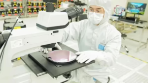
Jiufeng Mountain Laboratory announced a significant development in China’s semiconductor sector, the country’s first 100nm high-performance Gallium Nitride (GaN) fabrication Process Design Kit (PDK). The breakthrough follows on the heels of the lab’s recent unveiling of the world’s first 8-inch silicon-based nitrogen-polar GaN substrate (N-polar GaNOI). Jiufeng Mountain Laboratory has opted to bypass more conventional technology nodes below 150nm and proceed directly to a 100nm gate length. This approach delivers higher device cutoff frequencies and broader applicability across a range of uses, including DC to Ka-band millimeter-wave frequencies.
Researchers say they have also successfully reduced current collapse and lowered contact resistance, resulting in improved energy efficiency and power density. The use of silicon-based GaN allows for large wafer sizes, up to 8 inches.
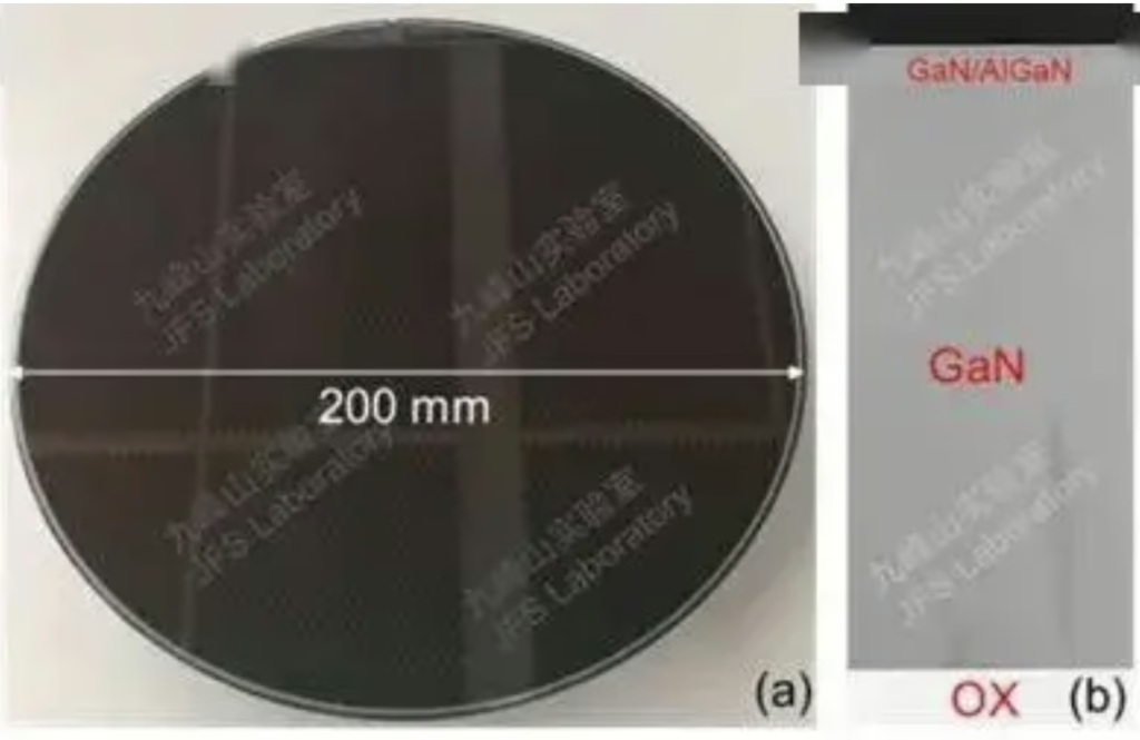
Earlier this month, the laboratory announced the world’s first 8-inch N-polar GaNOI substrate. N-polar GaN is seen by some industry experts as holding greater potential in high-frequency, high-power device applications than conventional gallium-polar GaN. The new substrate leverages silicon’s cost advantages, while delivering robust material performance and high yields suitable for large-scale commercial output.
GaN technology has long been celebrated in power electronics and high-frequency applications like 5G, radar, and satellite communications. However, its impact on advanced display technology, especially in emerging MicroLED displays, is just as noteworthy. MicroLED technology uses tiny GaN-based LEDs as individual pixels. By switching from smaller wafers to 8-inch (or larger) silicon-based GaN substrates, you pave the way for lower-cost, higher-volume manufacturing.
On the electronics side, GaN-based drivers offer faster switching and better power handling than traditional silicon components, making them ideal for demanding display applications such as large-format signage, high-refresh-rate panels, or even advanced AR/VR headsets. Because GaN transistors can handle high voltages and currents without significant heat or energy loss, they help reduce both power consumption and thermal issues.
As for the use of N-polar GaN, it can achieve higher electron velocities and potentially more efficient light emission than the conventional gallium-polar approach. That means GaN materials could eventually produce brighter pixels, cover a wider range of colors, or even improve overall device longevity. As MicroLED displays target ultra-high resolutions like 8K or above, optimizing each individual LED’s efficiency and manufacturing cost is critical. In the long run, having reliable, cost-effective GaN manufacturing at larger wafer sizes unlocks a path toward mainstream MicroLED products.