A large, international team of researchers headed by Junseok Jeong of Sejong University (Seoul, Korea) is developing an innovative method to fabricate highly flexible microLED arrays.

First, a little background information.
Currently, most flexible optoelectronic devices are fabricated using organic materials. The downside of even state-of-the-art organic materials is that they do not provide the best available optical and electrical properties – that claim belongs to inorganic semiconductor materials. A major downside to these better performing inorganic materials is that they are difficult to grow on flexible substrates.
One approach to addressing these issues is to grow semiconductors in the form of vertically aligned micro-structures. An array of such micro-structures, since it is composed of spatially separate devices, is found to offer an excellent geometry for use on flexible substrates. More specifically, the micro-structure approach that is the subject of this article is based on the use of vertically aligned gallium nitride (GaN) nano-structures in the form of nano-rods or nano-wires.
Although nano-structure-based semiconductors have the potential to be a successful means to implement flexible LEDs, there still remain materials related problems that need to be solved. A problem of particular significance is that the physical characteristics of the nanostructures are found to be affected by the physical characteristics of the underlying substrate. Stacking faults and strain near the interface are generated from bonds between nanostructures and the substrate. Other problems include the formation of an unintentional interfacial layer and contamination of the nanostructures via atom diffusion from the substrate. All of these problems may result in deterioration of LED performance.
Two additional factors need to be considered regarding the practical implementation of nano-structures.
First, the principle means to grow vertically aligned micro-structures is called remote epitaxy. Up to now, implementing remote epitaxy has required at least a near match between the lattice of the epilayer and the substrate. This, in turn, typically requires the use of high cost wafers as the substrate.
A second factor is that previous research has demonstrated that an Al2O3 wafer is a highly desirable substrate – except for the fact that it has a large in-plane lattice mismatch with GaN. The desirability of Al2O3 as a substrate is due to the fact that the material is highly compatible with the processing needed for conventional GaN growth and that it can be scaled to a large physical size.
Due to these two factors, there is a strong incentive to achieve the remote heteroepitaxy of vertical GaN nano-structures on Al2O3. (Remote heteroepitaxy is defined as a form of epitaxy in which one kind of crystal is grown upon the surface of a different type.) In an effort to achieve this goal, the researchers investigated means to deal with the lattice mismatch and the other undesirable influences related to the substrate.
The approach adopted by the researchers was based on the use of ultrathin graphene films. Such films consist of weakly bonded layers of hexagonally arranged carbon atoms bound together by strong covalent bonds. This allows graphene to provide desired flexibility with excellent mechanical strength – and the material is also chemically and physically inert at temperatures in excess of 1000°C. Given these material qualities, it is found that graphene serves to minimize the undesirable influences that relate to the substrate. A second feature of graphene is that it offers a small number of nucleation sites for GaN micro-structure growth. This, in turn, serves to enhance the three dimensional island growth of GaN micro-structures. Given this material quality, the graphene partially disconnects the growth of the lattice in the micro-structures from that of the lattice of the underlying Al2O3 substrate.
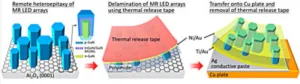
After growing the optimized micro-structure array, it can be removed from the graphene layer by use of a thermal release tape and transferred to another substrate – without the use of a process that destroys the sacrificial graphene layer during the removal process. The fabrication processes are illustrated in the figure below.
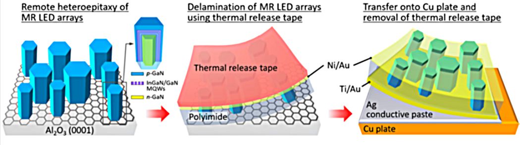 Schematics illustrating key procedures for fabricating the flexible LED, including remote heteroepitaxy of micro-structure (rod) LED arrays and transfer onto a conducting metal plate.
A recent article on this topic by the team was entitled “Remote heteroepitaxy of GaN microrod heterostructures for deformable light-emitting diodes and wafer recycle.” It was published in Science Advances, 3 Jun 2020, vol 6, issue 23. A copy of the article can be found here.
As described in the article, the LEDs were tested by “adhering them to curved surfaces as well as to materials that were subsequently twisted, bent and crumpled. The transferred micro-structure LEDs showed good electrical and electroluminescent performances with excellent flexibility. Stable, reliable electrical and electroluminescent properties were evidenced by repetitive bending cycles. The LEDs, fabricated from both the virgin and recycled wafers, reproducibly showed almost comparable LED performances.”
The researchers suggest that the reuse of wafer substrates has the potential to considerably reduce the material cost for LED production – without noticeable device degradation.
The researchers conclude their article with the statement that “We believe that the versatility of remote epitaxy will readily drive the epitaxy technology from yielding the rigid, brittle electronics into manufacturing the next-generation flexible, wearable electronics.” -Arthur Berman
Sejong University (Seoul, Republic of Korea), Young Joon Hong, [email protected]