MicroLEDs can be as small as 2 microns and bundled to produce a device of almost any size. These features can be considered some of the up-side of microLEDs fabricated using conventional technologies. One characteristic than can be considered a down-side is that LEDs made of thick film materials and fabricated on a wafer make them ridged and primarily suited for use on flat surfaces.

To make them better suited for use in flexible devices, it is necessary that the LEDs be minutely diced, lifted off the substrate upon which they were formed and attached to a flexible substrate. To address this need, researchers within the Department of Physics at The University of Texas (Richardson, TX) in collaboration with team members from several institutions in South Korea are developing a graphene-based method to fabricate microLEDs that are detachable from the substrate on which they are formed and then capable of being attached to a variety of other surfaces.
The method under development by the team is based on a technique called remote epitaxy. A recent article on this topic by the team is entitled “Remote heteroepitaxy of GaN microrod heterostructures for deformable light-emitting diodes and wafer recycle.” It was published in Science Advances 03 Jun 2020: Vol. 6, no. 23, eaaz5180. A copy of the article can be found here.
The new approach involves growing a thin layer of LED crystals on a substrate that is coated with a detachable, non-stick layer. Detailed information on the materials and processes used in the new method are contained in the article. A brief summary can be provided by paraphrasing the article as follows.
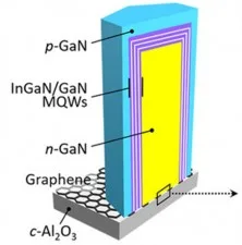
The researchers used remote heteroepitaxy of GaN microrod p-n junction arrays on a sapphire crystal (c-Al2O3) wafer substrate that was coated with a one atom thick layer of 2D graphene. The configuration of the device and the wafer are illustrated in the figure below.
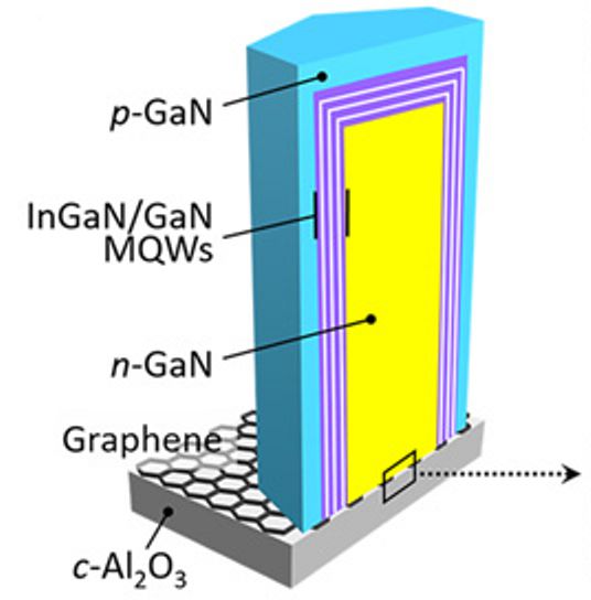 Cross-sectional schematic of microrod heterostructures grown on a graphene coated c-Al2O3 wafer.
The LEDs do not stick to the wafer because the graphene does not form chemical bonds with the LED material. With this the case, the researchers were able to detach the microLEDs from the wafer.
The laboratory methods used and the results obtained from testing the detachable microLEDs are also fully described in the article. The key take-aways are that the tests were carried out by adhering the microLEDs to curved surfaces, as well as to materials that were subsequently twisted, bent and crumpled. The results include that the electrical and light emitting properties of the microLEDs changed very little even after multiple bending cycles. In addition, cutting did not affect the electronic properties or other quality aspects of the transferred microLEDs.
From a manufacturing perspective, the new fabrication technique offers a real advantage. The advantage derives from the fact that it is possible to remove the microLEDs from the substrate multiple times without breaking or diminishing the functionality of the sapphire wafer or the graphene coating. More importantly, the experiments demonstrated that microLEDs fabricated from both virgin and recycled wafers reproducibly produced devices having undiminished performance. Since multiple re-use of substrates is possible, it follows that it should also be possible to reduce manufacturing costs.
In addition to microLED displays, flexible microLEDs have a variety of other possible uses. These include flexible lighting, clothing and wearable biomedical devices. More generally, the researcher state in their article that they believe that the new approach has the potential to enable the manufacturing technology used in the next generation flexible electronics. In support of the effort to make this happen, on-going studies conducted by the researchers include investigations into application of the new fabrication technique to other types of materials. – Arthur Berman
The University of Texas, Moon Kim, [email protected]