At SID Display Week last May, François Templier and Jeannet Bernard (Grenoble Université Alpes and CEA-LETI, Grenoble, France) presented Paper 18-3: “A New Approach for Fabricating High-Performance MicroLED Displays.” The paper is notable for being a clear tutorial on the challenges of tranfsferring millions of µLED chips from their native epiwafers to a display substrate with TFT backplane, and for introducing a very clever approach to easing those challenges.

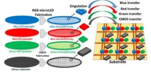
The brute-force approach is to use micro-transfer printing (µTP) or an alternative approach to separately transfer red, green, and blue µLED chips from their epiwafers to a TFT backplane, vastly increasing the pixel pitch in the process (Fig. 1). This is the concept used by AUO for the 7-inch tech demo it showed at Display Week 2018, but AUO simplified things by using only blue µLEDs, with color converters for green and red. Using this approach for a 4K TV screen would require the rapid transfer of 24 million µLED chips with near-perfect transfer yield. Even worse — or just as bad — is that making 65- or 75-inch panels would still require a Gen 10.5 fab with its astronomical capital expense.
 1. In the “brute force” approach to large-screen µLED fabrication, individual µLED chips are transferred to a TFT backplane. That’s 24 million chips for a 4K display. Fabrication time is orders of magnitude greater than is needed for practical commercial production. (Graphic: F. Templier and J. Bernard)
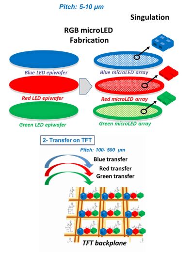
A more interesting approach is to use µTP to transfer not only an RGB trio of µLED chips for each pixel, but also a CMOS driving IC (Fig. 2). Each CMOS chip could drive one or more pixels. We are now transferring 32 million chips for a 4K display but we get a lot in return. The display substrate only has to supply X and Y conductors for power and signal, but no TFTs.
2. In the approach championed by X-Celeprint / XDC and others, pixel switching and driving is done with a CMOS IC that is transferred to the substrate along with the µLED chips. The substrate now contains only power and signal lines. With no TFTs, fabrication does not require an expensive fabs (Graphic: F. Templier and J. Bernard)
So the substrate is much simpler, much cheaper, and does not require an expensive fab. Templier and Bernard note that such substrates can be made with ink-jet or stencil printing, and can be made on a wide variety of rigid and flexible materials. Let’s say that again: Substrates of any size could be made in what amounts to a graphic arts studio, and would no longer require a multi-billion-dollar fab. In addition, the single-crystal pixel switches would provide stability and higher-quality images. In general, this is the approach used by X-Celeprint / XDC.
Veeco, working with X-Celeprint and others, has made a strong case that transferring the µLED chips to a mid-size substrate or interposer measuring 8 to 12 inches on a side, and then transferring the interposers to the final large-screen substrate, would significantly reduce the required number of transfers per display and reduce screen fabrication time.
Templier and Bernard have turned this idea around in a very clever way: They use the CMOS chip as a small interposer (Fig 3), and the µLED chips are transferred to the CMOS drivers at wafer scale. That is, the substrate is removed from an entire epiwafer’s worth of µLEDs, and the entire array is is transferred to the CMOS wafer. Repeat for the remaining two colors. Now, the RGB µLED-on-CMOS assemblies can be tested on-wafer, singulated, and transferred to the display substrate. We have just reduced the number of chip transfers by 75%. That’s significant.
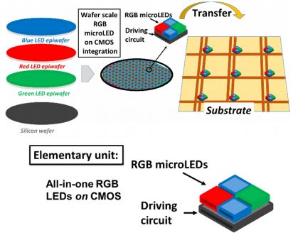 3. The authors’ innovation is to use the CMOS driving circuit as a small “interposer” for the µLED chips. The approach reduces the number of chip transfers by 75%. (Graphic: F. Templier and J. Bernard)
And the authors have reduced their technology to practice. A small demonstrator was shown in the LETI booth on the show floor, and the authors showed a photo in their presentation (Fig. 4). The making of affordable, large, µLED displays remains a challenging enterprise, but Templier and Bernard have taken a significant step in the right direction. (KW)
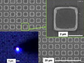 4. In this technology demo, 2µm integrated driver/pixels were positioned at a 5µm pitch. (Graphic: F. Templier and J. Bernard)
Ken Werner is Principal of Nutmeg Consultants, specializing in the display industry, manufacturing, technology, and applications, including mobile devices, automotive, and television. He consults for attorneys, investment analysts, and companies re-positioning themselves within the display industry or using displays in their products. He is the 2017 recipient of the Society for Information Display’s Lewis and Beatrice Winner Award. You can reach him at [email protected] or www.nutmegconsultants.com.