Researchers from Indian Institute of Technology Kanpur, India and University of Queensland, Australia have reported a major breakthrough in fabricating large area inkjet-printed organic light-emitting diodes (OLEDs) using a non-chlorinated, non-toxic solvent system.
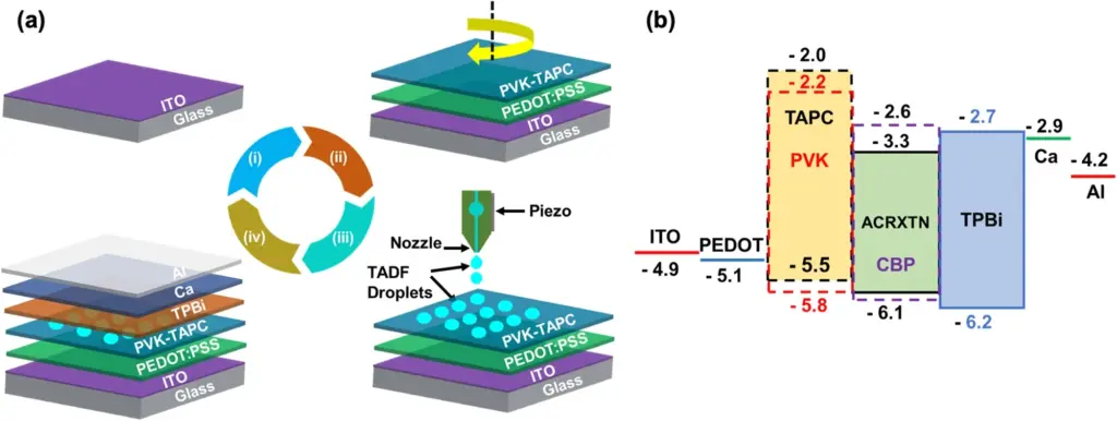
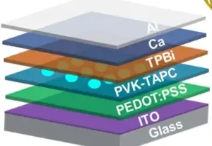
The team developed a thermally activated delayed fluorescence (TADF) ink using a novel binary solvent mixture of toluene and methyl benzoate. Unlike most solution-processable OLED inks that rely on toxic chlorinated solvents like chlorobenzene or chloroform, this new ink formulation utilizes greener, non-chlorinated solvents.
Through systematic optimization of ink rheology and waveform parameters, the researchers successfully inkjet printed the TADF emission layer in intricate patterns over large areas up to 80 x 80 mm2.
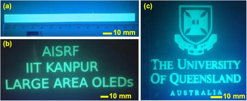
The OLED devices fabricated with inkjet-printed emission layers showed excellent performance, achieving brightness over 2000 cd/m2 and efficiencies comparable to control devices fabricated by spin coating. Impressively, this was accomplished at room temperature and ambient humidity, without the need for a cleanroom environment.
This work demonstrates for the first time an efficient, scalable technique for roll-to-roll fabrication of large area OLED displays and lighting panels using TADF inks. TADF materials enable high efficiency OLEDs without rare, expensive metals like iridium or platinum. The maskless inkjet printing technique also eliminates the need for expensive lithography steps.
According to the researchers, this technology could enable a new generation of large area, flexible OLED displays and lighting at much lower costs. The results represent a milestone towards economically feasible, eco-friendly manufacturing of OLEDs for next-generation flat panel displays, solid-state lighting, and other optoelectronic applications.
Reference
Kant, C., Shukla, A., McGregor, S.K.M. et al. Large area inkjet-printed OLED fabrication with solution-processed TADF ink. Nat Commun 14, 7220 (2023). https://doi.org/10.1038/s41467-023-43014-7