A team of researchers led by Professor of Experimental Physics Alan Dalton at the University of Sussex (Brighton, United Kingdom) is developing a silver nanowire-based technology for use in touchscreens. The focus of the new technology is the formation of extremely small pixel patterns. If successful, the new technology should allow the use of nanowire-based touch screens in conjunction with high definition LCD displays such as those commonly used in smartphones.
Previous research by Dalton’s group has shown that silver nanowire films can exceed the transmittance and conductivity of those made from Indium Tin Oxide (ITO), the widely used conventional material for such applications. The current work investigated some of the details related to patterning silver nanowire films to produce fine detailed electrode structures.
A recent publication by the team on this topic is entitled “Finite-size scaling in silver nanowire films: design considerations for practical devices.” It was published in Nanoscale, 8 (28). pp. 13701-13707.
In simple terms, lead author Matthew Large explains that “In this research we have applied a mathematical technique to work out the smallest subpixel size we can make without affecting the properties of our nanowire electrodes.”
More specifically, the article reports the “first application of finite-size scaling theory to nanostructured percolating networks, using silver nanowire (AgNW) films as a model system for experiment and simulation.”
Using this approach, the team studied the effect of systematic variation of the length distribution of the so-called percolating material. They “derived a design rule for the minimum viable feature size in a device pattern, relating it to parameters which can be derived from a transmittance-sheet resistance data series for the material in question.” The results of the new approach provide the researchers the information needed to tune the nanowires to meet the requirements of any given application.
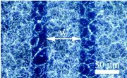
A microphotograph of the silver nanowire structure appears below.
The new and enhanced understanding of silver nanowire film formation has direct implications for the industrial adoption of silver nanowire electrodes in applications where small features are required. Such applications include single layer capacitive touch sensors, LCD and OLED displays.
The team is currently looking to apply its research results to commercial projects. The goal is to use silver nanowires in multi-touch sensor and to do so at a reduced production cost and energy usage as compared to those based on ITO. One of the commercial development efforts is reported to be in collaboration with industrial partner, M-SOLV (Oxford, United Kingdom). -Arthur Berman
University of Sussex, Alan Dalton, +44 (0)1273 678075,
[email protected]