The efficiency of electroluminescence in light emitting metal halide perovskite nanocrystals has been “limited by a lack of material strategies that can both suppress the formation of defects and enhance charge carrier confinement.” A large, international team of researchers is addressing this issue by developing new and improved materials using a “comprehensive defect suppression strategy.” If successful, such new materials could become important components in device applications that include LEDs.
The team was headed by Young-Hoon Kim within the Department of Materials Science and Engineering at Seoul National University (Seoul, Korea)
First a little background information.
One of the researchers in what would eventually become the team was studying a material called formamidinium lead bromide, a type of metal halide perovskite nanocrystal. Evaluations of green LEDs made with this material indicated that it was producing light more efficiently than predicted by theory. Due to this surprising result, the researcher had no choice but to conclude that the relationship between the structural, optical and light efficiency results was not properly understood. Eventually, a team of researchers formed to investigate this disconnect and develop a theory that could better explain the results. The team also conceived a series of follow up experiments that could be used to confirm any new theories.
A recent article by the team on this subject is entitled “Comprehensive defect suppression in perovskite nanocrystals for high-efficiency light-emitting diodes.” It was published in Nature Photonics (2021). A copy of the article is available for purchase and can be found here.
The team proceeded to develop a model using a method known as density functional theory. Using this model, the team determined that smaller perovskite nanocrystals have higher efficiency. One reason for this is that the probability of light generating events related to electrons finding a holes are much greater in smaller nanoparticles. On the other hand, reducing the size of a nanoparticle also increases its surface-to-volume ratio and this, in turn, allows for relatively more sites on the surface of the nanoparticle where defects can occur. The significance of this last point is that defects can cause electrons to lose energy and, eventually, lower material and device efficiency.
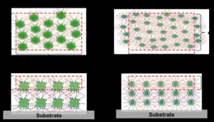
The team decided to investigate the effects of size in perovskite nanocrystals utilizing a technique called X-ray photoelectron spectroscopy. The results are a bit technical but can be summarized as follows.
In larger perovskite nanocrystals, a relatively small number of organic ligands were detected as compared to the inorganic backbone of the perovskite. Conversely, in smaller perovskite nanocrystals, a relatively large number of organic ligands were detected. This is illustrated in the figure below.
 A schematic illustration of the X-ray photoelectron spectroscopy measurements for: (upper left) larger perovskite nanocrystals (top view), (upper right) smaller perovskite nanocrystals (top view), (lower left) larger perovskite nanocrystals (side view) and (lower right) smaller perovskite nanocrystals (side view).
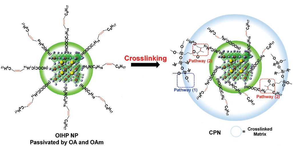
The team also found that a simple chemical substitution, replacing formamidinium with a larger organic cation called guanidinium, made the nanoparticles smaller. At the same time, the structural integrity of the material was preserved by the formation of a greater number of hydrogen bonds. Furthermore, that the addition of long chain acids and amines could be used to stabilize surface ions and that the addition of defect healing groups could be used to “heal” any vacancies that might form.
The result of all these considerations was the development of a material that was used to prototype what was described as a “highly efficient perovskite nanocrystal-based LED.” The prototype was found to have a current efficiency of 108?cd/A (external quantum efficiency of 23.4%), which rises to 205?cd/A (external quantum efficiency of 45.5%) with a hemispherical lens.
The bottom line of this research is that a new means of material design has been developed. This new means has the potential to improve perovskite nanoparticle material and LED device efficiency. -Arthur Berman
Seoul National University, Tae-Won Lee, [email protected]