A research collaboration between SmartKem and Prof. Xiaojun Guo’s group at Shanghai Jiao Tong University has yielded some interesting results. The goal was to develop a new monolithic integration approach to enable high-performance organic thin film transistors (OTFTs) to be directly fabricated onto MicroLED planes for active matrix MicroLED displays. The key innovation is an organic-last integration (OLI) technology using SmartKem’s printed electronic polymer materials to achieve superior OTFTs with properties critical for driving dense, high-resolution MicroLED displays.
The proposed OLI structure places the OTFT active matrix array directly on top of the MicroLED plane, reversing the typical configuration of having the light-emitting pixels on top. This is because the high temperatures (>350°C) required for traditional inorganic transistor materials like silicon would damage the MicroLED layers underneath. The organic semiconductors enable low temperature processing (<150°C) compatible with MicroLEDs. However, the non-planar surface of the MicroLED plane poses difficulties for depositing uniform organic films. The OLI approach addresses this through specific strategies:
- Thick polymer planarization layer to smooth the surface
- Metal shielding layer to prevent light influencing the OTFTs
- Post-OTFT via process that forms the electrical connection after fabricating the OTFT to avoid damage to the semiconductor layers
Together this enables high quality organic semiconductor/dielectric interfaces critical for stable, uniform, high-performance OTFTs on the MicroLED plane.
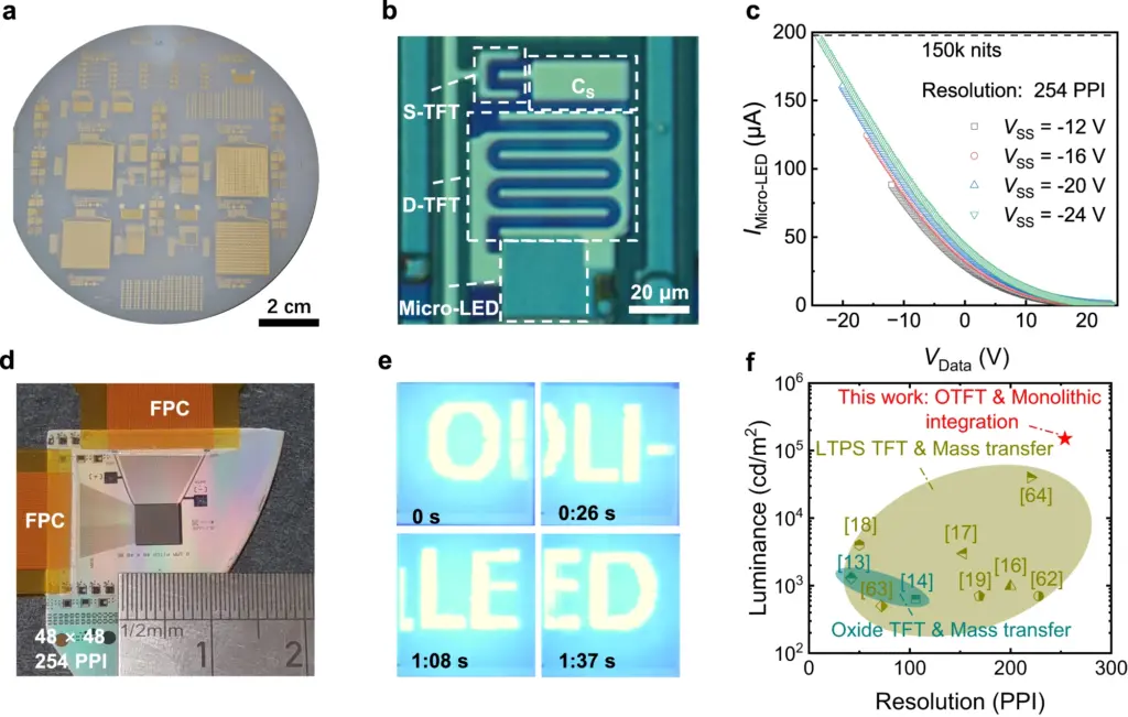
The OTFT uses a blended solution of a small molecule organic semiconductor (OSC) and polymer binder developed by SmartKem. This formulation improves crystallization control for superior mobility and low traps. A specialized self-assembled monolayer (SAM) on the source/drain electrodes reduces the injection barrier and improves OSC morphology. The hybrid organic gate dielectric with CYTOP and a polymer layer results in low leakage current and high capacitance.
These optimized OTFTs exhibit excellent electrical properties necessary for MicroLED displays:
- Large driving current approaching 1 mA
- Negligible leakage current
- High ON/OFF ratio near 10^10
- Operational stability under constant current and switching stress
- Environmental stability, retaining characteristics after storage in 84% humidity
The high current, low leakage, and stability enable bright, low power MicroLED operation. The TGBC structure allows short 3 μm channel length devices for high integration density. The customizable electronic inks facilitate scaling to large area circuits.
As for the post-OTFT via process, by fabricating the transistor before the via, the organic semiconductor layers remain pristine, avoiding damage from etching. This results in excellent uniformity across 4 inch wafers for the turn-on voltage and subthreshold swing. The scalability of the current delivers flexibility for circuit design. The reliability is proven through bias stress tests showing negligible threshold voltage shift after continuous operation.
Taken together, the OLI approach and tailored materials produce OTFTs with the uniformity, stability and precision needed for MicroLED integration, overcoming challenges with direct fabrication onto non-ideal surfaces.
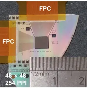
The multi-finger transistor layout provides sufficient current (>200 μA) in the 100 x 100 μm pixels. The resolution is 2-10x better than prior TFT-driven MicroLED displays while matching or exceeding their brightness. This establishes a new benchmark for monolithically integrated active matrix MicroLED technology.
Reference
Han, L., Ogier, S., Li, J., Sharkey, D., Yin, X., Baker, A., Carreras, A., Chang, F., Cheng, K., & Guo, X. (2023). Wafer-scale organic-on-III-V monolithic heterogeneous integration for active-matrix micro-LED displays. Nature Communications, 14(1), Article 1. https://doi.org/10.1038/s41467-023-42443-8