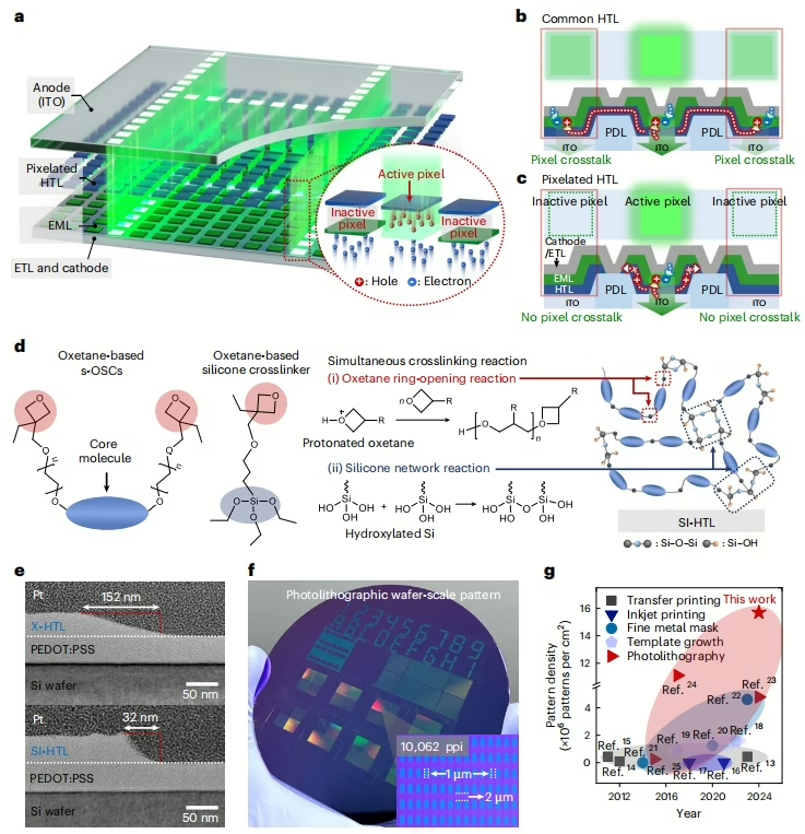
As displays become more densely packed with pixels, unwanted electrical interactions, known as crosstalk, can occur between adjacent pixels. This issue mainly arises because the layer responsible for transporting electrical holes (the hole transport layer) is shared among the pixels, leading to charge imbalances that degrade image quality. Traditional methods to address this problem involve increasing the thickness of this layer, but doing so can raise the driving voltage and reduce energy efficiency. Instead,
Korean researchers have developed a silicone-integrated small-molecule hole transport layer that is patterned with microlithography. This process allows for extremely precise structuring of the material at a microscopic scale, resulting in micro-pattern arrays that can achieve resolutions exceeding 10,000 pixels per inch on a six-inch wafer. By integrating this finely patterned layer into OLEDs, the device not only improves the charge balance within the emission layers but also significantly reduces electrical crosstalk between pixels. The innovative technique opens the door to high-definition displays that maintain excellent energy efficiency, making them suitable for a variety of modern electronic devices ranging from smart glasses to smartphones.

Recognizing that simply thickening this layer would lead to higher driving voltages and lower energy efficiency, the researchers set out to develop a new material, a silicone-integrated small-molecule hole transport layer. They synthesized this hybrid material and then applied microlithography. This process enabled them to create micro-pattern arrays with extremely high resolution on a six-inch wafer. Once the patterned layer was in place, they integrated it into OLED devices, fabricating micro-patterned OLED arrays. These devices were then rigorously tested to assess various performance parameters, including luminance and the degree of electrical crosstalk between pixels. The results showed that the patterned silicone-integrated hole transport layer not only maintained excellent charge balance within the emission layers but also significantly reduced unwanted electrical interactions between adjacent pixels, improving the overall efficiency and image quality of the OLED displays.
Reference
Kweon, H., Kim, S., Ha, B. et al. Microlithography of hole transport layers for high-resolution organic light-emitting diodes with reduced electrical crosstalk. Nat Electron 8, 66–74 (2025). https://doi.org/10.1038/s41928-024-01327-5

