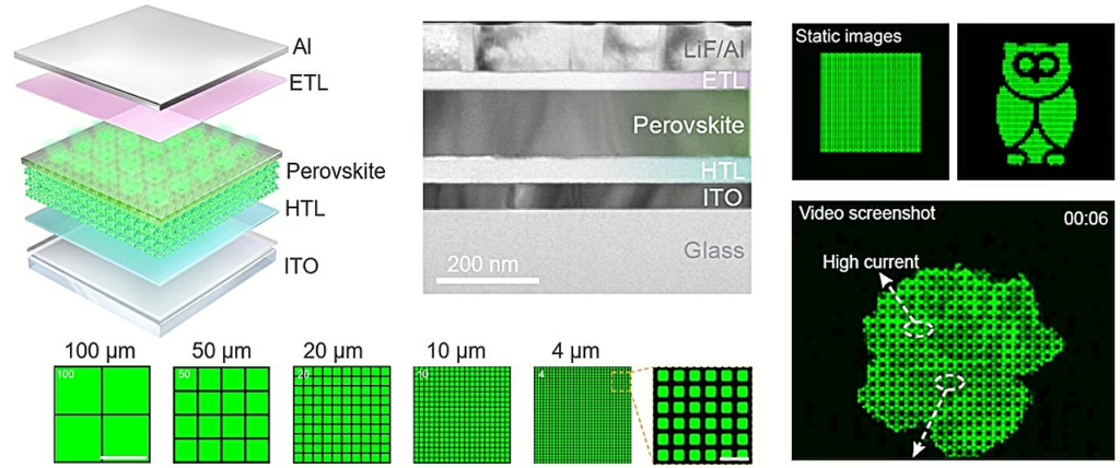
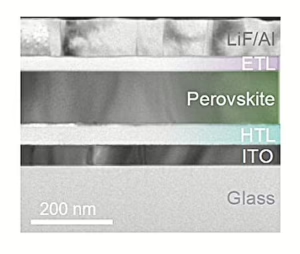
A team of researchers at the Technical Institute of Physics and Chemistry, Chinese Academy of Sciences has developed a novel method to grow high-quality perovskite thin films for MicroLEDs. The research could pave the way for ultrahigh-resolution displays that offer outstanding brightness and efficiency.

MicroLEDs, which measure just a few micrometers per pixel, promise superior energy efficiency, higher brightness, and sharper resolution compared to existing display technologies. Metal-halide perovskites are an attractive material choice for these tiny LEDs because they can combine efficient light emission with excellent long-range carrier transport, and they can also be manufactured using cost-effective solution-based processes. Nevertheless, conventional thin-film perovskites often suffer from inhomogeneous emission and surface instability during lithography, which undermine uniformity and complicate large-scale integration.
To resolve these issues, the researcher has introduced a remote epitaxial growth method. Traditional epitaxy involves growing a crystalline film directly on a crystalline substrate, ensuring alignment between the film and the substrate. In remote epitaxy, an ultrathin graphene interlayer—on the order of a subnanometer in thickness—is inserted between the substrate and the perovskite film. Although this graphene sheet provides a barrier that allows the perovskite film to be peeled away later, it is so thin that the substrate’s atomic arrangement can still guide the film’s crystallization. The result is a continuous, single-crystalline perovskite film that lacks the usual grain boundaries and features a pure out-of-plane crystallographic orientation. Once the film forms, it is straightforward to lift off, leaving behind a freestanding, flexible layer that can be transferred onto various electronic backplanes.
Eliminating problematic grain boundaries boosts the performance of perovskite-based MicroLEDs by reducing defect sites where charges can become trapped. Because charges move more efficiently in the defect-free film, these devices achieve higher brightness and better energy efficiency. According to the researchers, their remote-epitaxial perovskite films enable MicroLEDs with electroluminescence efficiencies above 16%, brightness levels reaching 4.0 × 10⁵ cd m−2, and a pixel size as small as 4 µm. This combination of parameters is crucial for emerging technologies such as near-eye displays used in augmented and virtual reality.
Beyond exceptional performance, an important advantage of these perovskite films lies in their ability to be lifted off from the original substrate and then attached to commercial electronic backplanes. The freestanding films can be independently controlled for each pixel, making them ideal for both static imagery and fully integrated video displays. Moreover, the manufacturing approach is compatible with stacking multiple perovskite compositions for full-color MicroLED arrays. The flexibility of this system also allows it to be monolithically integrated with advanced nanophotonic structures such as resonant metasurfaces or photonic crystals, which opens doors to ultracompact lasers and ultrafast LEDs.
The researchers anticipate that their remote epitaxy method will accelerate the commercialization of perovskite-based MicroLEDs, particularly for high-performance displays requiring superior resolution and brightness. Ongoing work on perovskite compositions, doping strategies, and device designs will likely further improve MicroLED efficiency, reliability, and integration.
Reference
Yuan, M., Feng, J., Li, H. et al. Remote epitaxial crystalline perovskites for ultrahigh-resolution micro-LED displays. Nat. Nanotechnol. (2025). https://doi.org/10.1038/s41565-024-01841-9

