Cornell University researchers, in collaboration with the Polish Academy of Sciences, have achieved a breakthrough in semiconductor technology with the development of a dual-sided dualtronic chip, capable of performing photonic and electronic functions simultaneously.
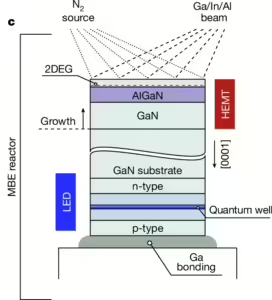
The development centers around gallium nitride (GaN), a wide-bandgap semiconductor known for its unique polarization properties. GaN’s distinct crystal structure allows for differing physical and chemical properties on each side of the wafer, enabling the researchers to exploit these characteristics. The team succeeded in integrating a high electron mobility transistor (HEMT) on one side and light-emitting diodes (LEDs) on the other—a first for any material, including silicon.
“No one has ever made active devices on both sides of a semiconductor before,” said van Deurzen. He explained that while silicon wafers are cubic and have identical properties on both sides, GaN’s polar nature creates a new degree of flexibility in designing devices.
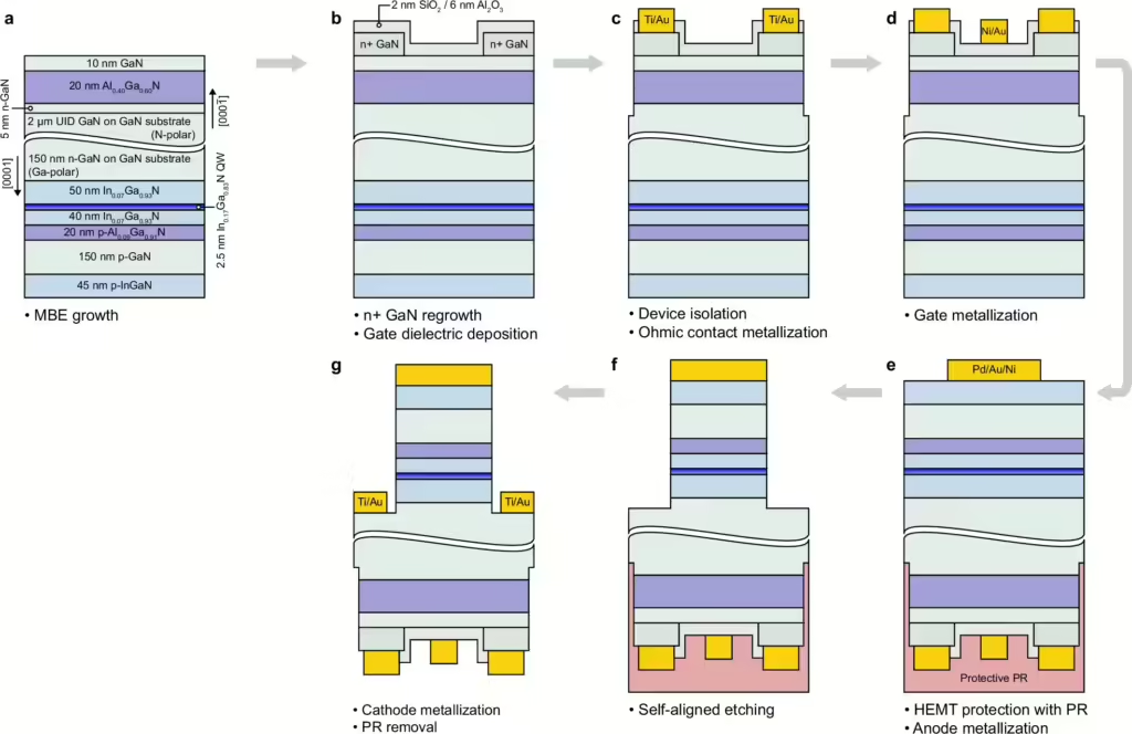
The project’s roots trace back to Cornell, where Jena, Xing, and former postdoctoral researcher Henryk Turski first conceived the concept. Working with a team in Poland, Turski grew GaN substrates, which were then shipped to Cornell for further processing. The fabrication process required overcoming significant challenges, particularly on the nitrogen polar face of the GaN wafer, which is more chemically reactive. The successful development of both a transistor and LED on opposite sides of the wafer marked a significant technological leap.
To test the device, the team had to develop new measurement techniques, including a crude but functional glass plate system to probe both sides of the wafer. Remarkably, the single HEMT device was able to drive the LED, switching it on and off at kilohertz frequencies, making it viable for applications like LED displays.
The dualtronic chip could immediately impact MicroLED displays, offering fewer components, a smaller footprint, and lower energy consumption. Jena likened the innovation to the multifunctional nature of modern smartphones, suggesting that by consolidating various functionalities into one chip, significant efficiencies could be realized.
Beyond displays, potential applications for the technology include the development of complementary metal-oxide-semiconductor (CMOS) devices and 5G and 6G communications systems. Additionally, the chips may serve in advanced applications like light-based LiFi communications.
Reference
van Deurzen, L., Kim, E., Pieczulewski, N. et al. Using both faces of polar semiconductor wafers for functional devices. Nature 634, 334–340 (2024). https://doi.org/10.1038/s41586-024-07983-z