At SID Display Week, in an aisle on the show floor, I had a brief conversation with Candice Brown-Elliott, Nouvoyance CEO and creator of the Pentile Matrix pixel configuration widely used in Samsung OLED displays.

She said that micro LED was the only disruptive technology she saw at Display Week. In addition to being a trusted colleague, Brown-Elliott has the rare gift of being both an insightful technical visionary and an effective engineer who doesn’t mind getting her knuckles scraped and her fingernails dirty. When Brown-Elliott says a technology is disruptive, I pay attention.
Just as remarkable as this technology’s potentially transformative nature is that micro LEDs (or microscale LEDs or µ-ILEDs) were not well known outside the relatively small community of people who work on them before Apple acquired LuxVue last year, at which point a much wider community started scrambling to learn about them.
Clearly, it would be very attractive to make phone, tablet, and TV displays from inorganic LEDs, but there has been no inexpensive way to assemble LED chips into RGB arrays of the appropriate density. If it were possible, such displays could be several times as efficient as OLEDs and have longer lifetimes.
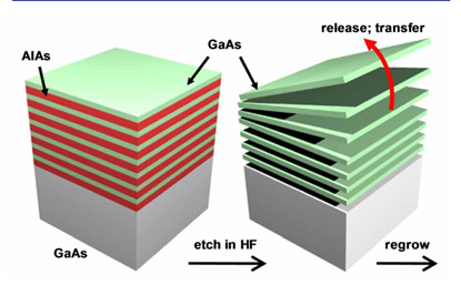
 Multilayer epitaxial lift-off (Graphic: John Rogers)So, the room was crowded when John Rogers – a professor at the University of Illinois and co-founder of and technology advisor to X-Celeprint – presented a Monday seminar entitled “Microscale LEDs for Multifunctional Display Systems.” What Rogers and his colleagues, along with a handful of other micro-LED companies, have learned to do is is initiate the epitaxial growth of AlInGaP LEDs on recyclable GaAs wafers. Rogers described a process for making multiple layers of LEDs with sacrificial layers in between that allow the layers to be lifted off That’s impressive but it solves only half the problem. If we went no farther, we could no more than make expensive wafer-sized displays.
The second part of the solution was covered by Chris Bower, CTO of X-Celeprint (Cork, Ireland), who described the company’s technology for performing transfer printing of the chips using elastomeric stamps utilizing peel-rate-dependent adhesion. To oversimplify shamelessly, if you place the stamp on the layer of chips and peel it off quickly the chips adhere to the stamp. Impress the stamp on the target substrate and peel it off slowly, the chips adhere to the target. This is also impressive, but it still doesn’t created LED arrays any larger than the original lattice-matched array.
As it turns out, it is relatively simple to impose patterns on the stamps that result in picking up every 10th, 20th, or nth LED before depositing them on the substrate. In this way, you can go from the dense array of the original wafer to a sparse array on the target substrate. In principal, this allows you to make µ-ILED displays of virtually any diagonal. Bower said that X-Celeprint has made 150-mm stamps. Making larger ones is just a matter of engineering, he said, not science.
Now, is it obvious to that if you can transfer-print u-iLEDs you can also transfer-print CMOS switching circuits and no longer worry about the instability issues of a-Si and IGZO TFTs or the scalability issues of LTPS? Well, even if it’s not obvious, Rogers discussed it in his seminar. In fact, you can transfer print many kinds of “chiplets,” and even assemble them in three-dimensional structures. Displays are only one application of the technology.
The first µ-ILED display we see in a commercial product may very well come from LuxVue and appear in an Apple iWatch next year.
Looking farther forward, is it possible that µ-ILED, not OLED, will become the universal display that replaces LCD? All of us in the display community should be thinking about that question, and thinking hard. – Ken Werner

